C8051F320DK Silicon Laboratories Inc, C8051F320DK Datasheet - Page 203
C8051F320DK
Manufacturer Part Number
C8051F320DK
Description
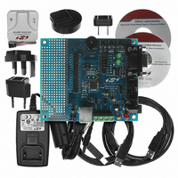
DEV KIT FOR C8051F320/F321
Manufacturer
Silicon Laboratories Inc
Type
MCUr
Specifications of C8051F320DK
Contents
Evaluation Board, Power Supply, USB Cables, Adapter and Documentation
Processor To Be Evaluated
C8051F320/F321
Interface Type
USB
Silicon Manufacturer
Silicon Labs
Core Architecture
8051
Silicon Core Number
C8051F320
Silicon Family Name
C8051F32x
Lead Free Status / RoHS Status
Contains lead / RoHS non-compliant
For Use With/related Products
Silicon Laboratories C8051F320, C8051F321
Lead Free Status / Rohs Status
Lead free / RoHS Compliant
Other names
336-1260
Available stocks
Company
Part Number
Manufacturer
Quantity
Price
Company:

Part Number:
C8051F320DK
Manufacturer:
SiliconL
Quantity:
4


Bit 7:
Bit 6:
Bit 5:
Bit 4:
Bit 3:
Bit 2:
Bit 1:
Bit 0:
*Note:
SPIBSY
Bit7
R
SPIBSY: SPI Busy (read only).
This bit is set to logic 1 when a SPI transfer is in progress (Master or slave Mode).
MSTEN: Master Mode Enable.
0: Disable master mode. Operate in slave mode.
1: Enable master mode. Operate as a master.
CKPHA: SPI0 Clock Phase.
This bit controls the SPI0 clock phase.
0: Data centered on first edge of SCK period.*
1: Data centered on second edge of SCK period.*
CKPOL: SPI0 Clock Polarity.
This bit controls the SPI0 clock polarity.
0: SCK line low in idle state.
1: SCK line high in idle state.
SLVSEL: Slave Selected Flag (read only).
This bit is set to logic 1 whenever the NSS pin is low indicating SPI0 is the selected slave. It
is cleared to logic 0 when NSS is high (slave not selected). This bit does not indicate the
instantaneous value at the NSS pin, but rather a de-glitched version of the pin input.
NSSIN: NSS Instantaneous Pin Input (read only).
This bit mimics the instantaneous value that is present on the NSS port pin at the time that
the register is read. This input is not de-glitched.
SRMT: Shift Register Empty (Valid in Slave Mode, read only).
This bit will be set to logic 1 when all data has been transferred in/out of the shift register,
and there is no new information available to read from the transmit buffer or write to the
receive buffer. It returns to logic 0 when a data byte is transferred to the shift register from
the transmit buffer or by a transition on SCK.
NOTE: SRMT = 1 when in Master Mode.
RXBMT: Receive Buffer Empty (Valid in Slave Mode, read only).
This bit will be set to logic 1 when the receive buffer has been read and contains no new
information. If there is new information available in the receive buffer that has not been read,
this bit will return to logic 0.
NOTE: RXBMT = 1 when in Master Mode.
sampled one SYSCLK before the end of each data bit, to provide maximum settling time for the slave
device. See Table 18.1 for timing parameters.
In slave mode, data on MOSI is sampled in the center of each data bit. In master mode, data on MISO is
MSTEN
R/W
Bit6
SFR Definition 18.1. SPI0CFG: SPI0 Configuration
CKPHA
R/W
Bit5
CKPOL
R/W
Bit4
SLVSEL
Rev. 1.4
Bit3
R
NSSIN
Bit2
R
SRMT
Bit1
R
C8051F320/1
SFR Address: 0xA1
RXBMT
Bit0
R
Reset Value
00000111
203
Related parts for C8051F320DK
Image
Part Number
Description
Manufacturer
Datasheet
Request
R

Part Number:
Description:
SMD/C°/SINGLE-ENDED OUTPUT SILICON OSCILLATOR
Manufacturer:
Silicon Laboratories Inc
Part Number:
Description:
Manufacturer:
Silicon Laboratories Inc
Datasheet:
Part Number:
Description:
N/A N/A/SI4010 AES KEYFOB DEMO WITH LCD RX
Manufacturer:
Silicon Laboratories Inc
Datasheet:
Part Number:
Description:
N/A N/A/SI4010 SIMPLIFIED KEY FOB DEMO WITH LED RX
Manufacturer:
Silicon Laboratories Inc
Datasheet:
Part Number:
Description:
N/A/-40 TO 85 OC/EZLINK MODULE; F930/4432 HIGH BAND (REV E/B1)
Manufacturer:
Silicon Laboratories Inc
Part Number:
Description:
EZLink Module; F930/4432 Low Band (rev e/B1)
Manufacturer:
Silicon Laboratories Inc
Part Number:
Description:
I°/4460 10 DBM RADIO TEST CARD 434 MHZ
Manufacturer:
Silicon Laboratories Inc
Part Number:
Description:
I°/4461 14 DBM RADIO TEST CARD 868 MHZ
Manufacturer:
Silicon Laboratories Inc
Part Number:
Description:
I°/4463 20 DBM RFSWITCH RADIO TEST CARD 460 MHZ
Manufacturer:
Silicon Laboratories Inc
Part Number:
Description:
I°/4463 20 DBM RADIO TEST CARD 868 MHZ
Manufacturer:
Silicon Laboratories Inc
Part Number:
Description:
I°/4463 27 DBM RADIO TEST CARD 868 MHZ
Manufacturer:
Silicon Laboratories Inc
Part Number:
Description:
I°/4463 SKYWORKS 30 DBM RADIO TEST CARD 915 MHZ
Manufacturer:
Silicon Laboratories Inc
Part Number:
Description:
N/A N/A/-40 TO 85 OC/4463 RFMD 30 DBM RADIO TEST CARD 915 MHZ
Manufacturer:
Silicon Laboratories Inc
Part Number:
Description:
I°/4463 20 DBM RADIO TEST CARD 169 MHZ
Manufacturer:
Silicon Laboratories Inc