C8051F320DK Silicon Laboratories Inc, C8051F320DK Datasheet - Page 3
C8051F320DK
Manufacturer Part Number
C8051F320DK
Description
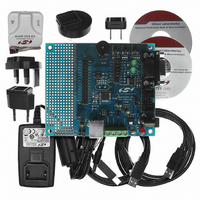
DEV KIT FOR C8051F320/F321
Manufacturer
Silicon Laboratories Inc
Type
MCUr
Specifications of C8051F320DK
Contents
Evaluation Board, Power Supply, USB Cables, Adapter and Documentation
Processor To Be Evaluated
C8051F320/F321
Interface Type
USB
Silicon Manufacturer
Silicon Labs
Core Architecture
8051
Silicon Core Number
C8051F320
Silicon Family Name
C8051F32x
Lead Free Status / RoHS Status
Contains lead / RoHS non-compliant
For Use With/related Products
Silicon Laboratories C8051F320, C8051F321
Lead Free Status / Rohs Status
Lead free / RoHS Compliant
Other names
336-1260
Available stocks
Company
Part Number
Manufacturer
Quantity
Price
Company:

Part Number:
C8051F320DK
Manufacturer:
SiliconL
Quantity:
4


Table of Contents
1. System Overview.................................................................................................... 15
2. Absolute Maximum Ratings .................................................................................. 27
3. Global Electrical Characteristics .......................................................................... 28
4. Pinout and Package Definitions............................................................................ 30
5. 10-Bit ADC (ADC0).................................................................................................. 39
6. Voltage Reference .................................................................................................. 55
7. Comparators ......................................................................................................... 57
8. Voltage Regulator (REG0)...................................................................................... 67
9. CIP-51 Microcontroller .......................................................................................... 71
1.1. CIP-51™ Microcontroller Core.......................................................................... 18
1.2. On-Chip Memory............................................................................................... 19
1.3. Universal Serial Bus Controller ......................................................................... 20
1.4. Voltage Regulator ............................................................................................. 21
1.5. On-Chip Debug Circuitry................................................................................... 21
1.6. Programmable Digital I/O and Crossbar ........................................................... 22
1.7. Serial Ports ....................................................................................................... 23
1.8. Programmable Counter Array ........................................................................... 23
1.9. 10-Bit Analog to Digital Converter..................................................................... 24
1.10.Comparators..................................................................................................... 25
5.1. Analog Multiplexer ............................................................................................ 40
5.2. Temperature Sensor ......................................................................................... 41
5.3. Modes of Operation .......................................................................................... 43
5.4. Programmable Window Detector ...................................................................... 50
8.1. Regulator Mode Selection................................................................................. 67
8.2. VBUS Detection ................................................................................................ 67
9.1. Instruction Set ................................................................................................... 72
9.2. Memory Organization........................................................................................ 77
1.1.1. Fully 8051 Compatible.............................................................................. 18
1.1.2. Improved Throughput ............................................................................... 18
1.1.3. Additional Features .................................................................................. 18
5.3.1. Starting a Conversion............................................................................... 43
5.3.2. Tracking Modes........................................................................................ 44
5.3.3. Settling Time Requirements ..................................................................... 45
5.4.1. Window Detector In Single-Ended Mode ................................................. 52
5.4.2. Window Detector In Differential Mode...................................................... 53
9.1.1. Instruction and CPU Timing ..................................................................... 72
9.1.2. MOVX Instruction and Program Memory ................................................. 73
9.2.1. Program Memory...................................................................................... 77
9.2.2. Data Memory............................................................................................ 78
9.2.3. General Purpose Registers ...................................................................... 78
9.2.4. Bit Addressable Locations........................................................................ 78
9.2.5. Stack ....................................................................................................... 78
9.2.6. Special Function Registers....................................................................... 79
Rev. 1.4
C8051F320/1
3
Related parts for C8051F320DK
Image
Part Number
Description
Manufacturer
Datasheet
Request
R

Part Number:
Description:
SMD/C°/SINGLE-ENDED OUTPUT SILICON OSCILLATOR
Manufacturer:
Silicon Laboratories Inc
Part Number:
Description:
Manufacturer:
Silicon Laboratories Inc
Datasheet:
Part Number:
Description:
N/A N/A/SI4010 AES KEYFOB DEMO WITH LCD RX
Manufacturer:
Silicon Laboratories Inc
Datasheet:
Part Number:
Description:
N/A N/A/SI4010 SIMPLIFIED KEY FOB DEMO WITH LED RX
Manufacturer:
Silicon Laboratories Inc
Datasheet:
Part Number:
Description:
N/A/-40 TO 85 OC/EZLINK MODULE; F930/4432 HIGH BAND (REV E/B1)
Manufacturer:
Silicon Laboratories Inc
Part Number:
Description:
EZLink Module; F930/4432 Low Band (rev e/B1)
Manufacturer:
Silicon Laboratories Inc
Part Number:
Description:
I°/4460 10 DBM RADIO TEST CARD 434 MHZ
Manufacturer:
Silicon Laboratories Inc
Part Number:
Description:
I°/4461 14 DBM RADIO TEST CARD 868 MHZ
Manufacturer:
Silicon Laboratories Inc
Part Number:
Description:
I°/4463 20 DBM RFSWITCH RADIO TEST CARD 460 MHZ
Manufacturer:
Silicon Laboratories Inc
Part Number:
Description:
I°/4463 20 DBM RADIO TEST CARD 868 MHZ
Manufacturer:
Silicon Laboratories Inc
Part Number:
Description:
I°/4463 27 DBM RADIO TEST CARD 868 MHZ
Manufacturer:
Silicon Laboratories Inc
Part Number:
Description:
I°/4463 SKYWORKS 30 DBM RADIO TEST CARD 915 MHZ
Manufacturer:
Silicon Laboratories Inc
Part Number:
Description:
N/A N/A/-40 TO 85 OC/4463 RFMD 30 DBM RADIO TEST CARD 915 MHZ
Manufacturer:
Silicon Laboratories Inc
Part Number:
Description:
I°/4463 20 DBM RADIO TEST CARD 169 MHZ
Manufacturer:
Silicon Laboratories Inc