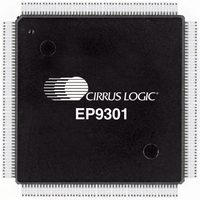
EP9301-CQZ Cirrus Logic Inc, EP9301-CQZ Datasheet - Page 425

EP9301-CQZ
Manufacturer Part Number
EP9301-CQZ
Description
IC ARM9 SOC PROCESSOR 208LQFP
Manufacturer
Cirrus Logic Inc
Series
EP9r
Specifications of EP9301-CQZ
Core Size
16/32-Bit
Peripherals
AC'97, DMA, I²:S, LED, MaverickKey, POR, PWM, WDT
Core Processor
ARM9
Speed
166MHz
Connectivity
EBI/EMI, Ethernet, I²C, IrDA, SPI, UART/USART, USB
Number Of I /o
19
Program Memory Type
ROMless
Ram Size
32K x 8
Voltage - Supply (vcc/vdd)
1.65 V ~ 3.6 V
Data Converters
A/D 5x12b
Oscillator Type
External
Operating Temperature
0°C ~ 70°C
Package / Case
208-TQFP, 208-VQFP
Controller Family/series
(ARM9)
No. Of I/o's
19
Ram Memory Size
16MB
Cpu Speed
166MHz
No. Of Timers
4
Digital Ic Case Style
TQFP
Embedded Interface Type
SPI
Rohs Compliant
Yes
Processor Series
EP93xx
Core
ARM920T
Data Bus Width
32 bit
3rd Party Development Tools
MDK-ARM, RL-ARM, ULINK2
Lead Free Status / RoHS Status
Lead free / RoHS Compliant
Eeprom Size
-
Program Memory Size
-
Lead Free Status / Rohs Status
Details
Other names
598-1136
Available stocks
Company
Part Number
Manufacturer
Quantity
Price
Company:
Part Number:
EP9301-CQZ
Manufacturer:
CIRRUS
Quantity:
3 390
Part Number:
EP9301-CQZ
Manufacturer:
CIRRUSLOGIC
Quantity:
20 000
Company:
Part Number:
EP9301-CQZR
Manufacturer:
Cirrus Logic Inc
Quantity:
10 000
- Current page: 425 of 824
- Download datasheet (13Mb)
CONTROL
DS785UM1
ETDP
31
15
Address:
Definition:
Bit Descriptions:
30
14
TM
Channel Base Address + 0x002C
Channel Base Address + 0x003C
Channel Base Address + 0x0028
Channel Base Address + 0x0030
Channel Base Address + 0x0034
Channel Base Address + 0x0038
29
13
PWSC
SAH
28
12
Channel Base Address + 0x0000 - Read/Write
This is the Channel Control Register. Used to configure the DMA M2M
Channel. All control bits should be programmed before the ENABLE bit is set.
RSVD:
STALLIntEn:
SCT:
Offset
DAH
27
11
Note:See
Note:* Write this location once to clear the bit (see Interrupt/Status register description
Table 10-8. PPALLOC Register Reset Values (Continued)
26
10
for which bits this rule applies to).
PW
Table 10-3
25
9
Copyright 2007 Cirrus Logic
NO_HDSK
Reserved. Unknown During Read.
Setting this bit to “1” enables the generation of the STALL
interrupt in the STALL State of the DMA Channel State
machine. Setting this bit to “0” disables generation of the
STALL Interrupt.
Source Copy Transfer. This bit is used to set up a block
transfer from 1 memory source location. If SCT = 1, then
one word is read from the source memory location and
copied to a block of memory (the number of destination
locations written to is determined by BCR). If SCT = 0 then
the source address increments as normal after each
successful transfer as determined by the transfer size (this
is the default setting). In order to use this feature the
SAR_BASEx and DAR_BASEx registers must contain
word-aligned addresses - the DMA will ignore the 2 LSB’s
SAR_CURRENT1
DAR_CURRENT0
DAR_CURRENT1
24
for Channel Base Addresses
8
DAR_BASE0
DAR_BASE1
Reserved
Name
23
7
BWC
RSS
22
6
NFBintEn
Access
21
5
R/W
R/W
RO
RO
RO
START
20
4
DREQP
Bits
32
32
32
32
32
ENABLE
19
3
Reset Value
DONEIntEn
RSVD
18
0
0
0
0
0
EP93xx User’s Guide
2
DMA Controller
DACKP
SCT
17
1
STALLIntEn
ETDP
16
10-31
0
10
Related parts for EP9301-CQZ
Image
Part Number
Description
Manufacturer
Datasheet
Request
R

Part Number:
Description:
32-Bit Microcontroller IC
Manufacturer:
Cirrus Logic Inc
Datasheet:

Part Number:
Description:
IC ARM920T MCU 166MHZ 208-LQFP
Manufacturer:
Cirrus Logic Inc
Datasheet:

Part Number:
Description:
IC ARM920T MCU 166MHZ 208-LQFP
Manufacturer:
Cirrus Logic Inc
Datasheet:

Part Number:
Description:
Development Kit
Manufacturer:
Cirrus Logic Inc
Datasheet:

Part Number:
Description:
Development Kit
Manufacturer:
Cirrus Logic Inc
Datasheet:

Part Number:
Description:
High-efficiency PFC + Fluorescent Lamp Driver Reference Design
Manufacturer:
Cirrus Logic Inc
Datasheet:

Part Number:
Description:
Development Kit
Manufacturer:
Cirrus Logic Inc
Datasheet:

Part Number:
Description:
Development Kit
Manufacturer:
Cirrus Logic Inc
Datasheet:

Part Number:
Description:
Development Kit
Manufacturer:
Cirrus Logic Inc
Datasheet:

Part Number:
Description:
Development Kit
Manufacturer:
Cirrus Logic Inc
Datasheet:

Part Number:
Description:
Development Kit
Manufacturer:
Cirrus Logic Inc
Datasheet:

Part Number:
Description:
Development Kit
Manufacturer:
Cirrus Logic Inc
Datasheet:

Part Number:
Description:
Ref Bd For Speakerbar MSA & DSP Products
Manufacturer:
Cirrus Logic Inc


