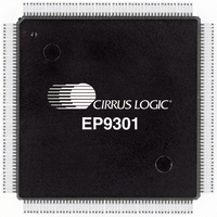
EP9301-CQZ Cirrus Logic Inc, EP9301-CQZ Datasheet - Page 718

EP9301-CQZ
Manufacturer Part Number
EP9301-CQZ
Description
IC ARM9 SOC PROCESSOR 208LQFP
Manufacturer
Cirrus Logic Inc
Series
EP9r
Specifications of EP9301-CQZ
Core Size
16/32-Bit
Peripherals
AC'97, DMA, I²:S, LED, MaverickKey, POR, PWM, WDT
Core Processor
ARM9
Speed
166MHz
Connectivity
EBI/EMI, Ethernet, I²C, IrDA, SPI, UART/USART, USB
Number Of I /o
19
Program Memory Type
ROMless
Ram Size
32K x 8
Voltage - Supply (vcc/vdd)
1.65 V ~ 3.6 V
Data Converters
A/D 5x12b
Oscillator Type
External
Operating Temperature
0°C ~ 70°C
Package / Case
208-TQFP, 208-VQFP
Controller Family/series
(ARM9)
No. Of I/o's
19
Ram Memory Size
16MB
Cpu Speed
166MHz
No. Of Timers
4
Digital Ic Case Style
TQFP
Embedded Interface Type
SPI
Rohs Compliant
Yes
Processor Series
EP93xx
Core
ARM920T
Data Bus Width
32 bit
3rd Party Development Tools
MDK-ARM, RL-ARM, ULINK2
Lead Free Status / RoHS Status
Lead free / RoHS Compliant
Eeprom Size
-
Program Memory Size
-
Lead Free Status / Rohs Status
Details
Other names
598-1136
Available stocks
Company
Part Number
Manufacturer
Quantity
Price
Company:
Part Number:
EP9301-CQZ
Manufacturer:
CIRRUS
Quantity:
3 390
Part Number:
EP9301-CQZ
Manufacturer:
CIRRUSLOGIC
Quantity:
20 000
Company:
Part Number:
EP9301-CQZR
Manufacturer:
Cirrus Logic Inc
Quantity:
10 000
- Current page: 718 of 824
- Download datasheet (13Mb)
23
23-6
Synchronous Serial Port
EP93xx User’s Guide
In this configuration, during idle periods:
If the SSP is enabled and there is valid data within the transmit FIFO, the start of
transmission is signified by the SFRMOUT master signal being driven LOW. This causes
slave data to be enabled onto the SSPRXD input line of the master. The master SSPTXD
output pad is enabled.
One half SCLKOUT period later, valid master data is transferred to the SSPTXD pin. Now
that both the master and slave data have been set, the SCLKOUT master clock pin goes
HIGH after one further half SCLKOUT period.
The data is now captured on the rising edges, and is propagated on the falling edges, of the
SCLKOUT signal.
In the case of a single word transmission, after all bits of the data word have been
transferred, the SFRMOUT line is returned to its idle HIGH state one SCLKOUT period after
the last bit has been captured.
However, in the case of continuous back-to-back transmissions, the SFRMOUT signal must
be pulsed HIGH between each data word transfer. This is because the slave select pin
freezes the data in its serial peripheral register and does not allow it to be altered if the SPH
bit is logic zero. Therefore the master device must raise the SFRMIN pin of the slave device
between each data transfer to enable the serial peripheral data write. On completion of the
continuous transfer, the SFRMOUT pin is returned to its idle state one SCLKOUT period after
the last bit has been captured.
• the SCLKOUT signal is forced LOW
• SFRMOUT is forced HIGH
• the transmit data line SSPTXD is arbitrarily forced LOW
• when the SSP is configured as a master, the SSPCTLOE line is driven LOW, enabling
• when the SSP is configured as a slave, the SSPCTLOE line is driven HIGH, disabling
SSPOE (=0)
the SCLKOUT pad (active LOW enable)
the SCLKOUT pad (active LOW enable).
SCLKOUT /
SCLKIN
SFRMOUT /
SFRMIN
SSPRXD
SSPTXD
Figure 23-4. Motorola SPI Frame Format (Continuous Transfer)
LS B
LS B
M SB
Copyright 2007 Cirrus Logic
M SB
with SPO=0 and SPH=0
4 t o 16 bi t s
LSB
LSB
M SB
M SB
DS785UM1
Related parts for EP9301-CQZ
Image
Part Number
Description
Manufacturer
Datasheet
Request
R

Part Number:
Description:
32-Bit Microcontroller IC
Manufacturer:
Cirrus Logic Inc
Datasheet:

Part Number:
Description:
IC ARM920T MCU 166MHZ 208-LQFP
Manufacturer:
Cirrus Logic Inc
Datasheet:

Part Number:
Description:
IC ARM920T MCU 166MHZ 208-LQFP
Manufacturer:
Cirrus Logic Inc
Datasheet:

Part Number:
Description:
Development Kit
Manufacturer:
Cirrus Logic Inc
Datasheet:

Part Number:
Description:
Development Kit
Manufacturer:
Cirrus Logic Inc
Datasheet:

Part Number:
Description:
High-efficiency PFC + Fluorescent Lamp Driver Reference Design
Manufacturer:
Cirrus Logic Inc
Datasheet:

Part Number:
Description:
Development Kit
Manufacturer:
Cirrus Logic Inc
Datasheet:

Part Number:
Description:
Development Kit
Manufacturer:
Cirrus Logic Inc
Datasheet:

Part Number:
Description:
Development Kit
Manufacturer:
Cirrus Logic Inc
Datasheet:

Part Number:
Description:
Development Kit
Manufacturer:
Cirrus Logic Inc
Datasheet:

Part Number:
Description:
Development Kit
Manufacturer:
Cirrus Logic Inc
Datasheet:

Part Number:
Description:
Development Kit
Manufacturer:
Cirrus Logic Inc
Datasheet:

Part Number:
Description:
Ref Bd For Speakerbar MSA & DSP Products
Manufacturer:
Cirrus Logic Inc


