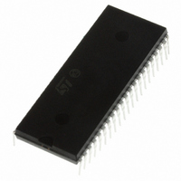
ST72F324BJ6B6 STMicroelectronics, ST72F324BJ6B6 Datasheet - Page 103

ST72F324BJ6B6
Manufacturer Part Number
ST72F324BJ6B6
Description
MCU 8BIT 32KB FLASH/ROM 42-SDIP
Manufacturer
STMicroelectronics
Series
ST7r
Datasheet
1.ST72F324BJ6B6.pdf
(193 pages)
Specifications of ST72F324BJ6B6
Core Processor
ST7
Core Size
8-Bit
Speed
8MHz
Connectivity
SCI, SPI
Peripherals
LVD, POR, PWM, WDT
Number Of I /o
32
Program Memory Size
32KB (32K x 8)
Program Memory Type
FLASH
Ram Size
1K x 8
Voltage - Supply (vcc/vdd)
3.8 V ~ 5.5 V
Data Converters
A/D 12x10b
Oscillator Type
Internal
Operating Temperature
-40°C ~ 85°C
Package / Case
42-SDIP (0.600", 15.24mm)
Controller Family/series
ST7
No. Of I/o's
32
Ram Memory Size
1KB
Cpu Speed
8MHz
No. Of Timers
2
Embedded Interface Type
SCI, SPI
No. Of Pwm Channels
3
Processor Series
ST72F3x
Core
ST7
Data Bus Width
8 bit
Data Ram Size
1 KB
Interface Type
SCI, SPI
Maximum Clock Frequency
8 MHz
Number Of Programmable I/os
32
Number Of Timers
3
Maximum Operating Temperature
+ 85 C
Mounting Style
Through Hole
Development Tools By Supplier
ST7232X-EVAL, ST7MDT20-DVP3, ST7MDT20J-EMU3, STX-RLINK
Minimum Operating Temperature
- 40 C
On-chip Adc
10 bit, 12 Channel
For Use With
497-6421 - BOARD EVAL DGTL BATT CHGR DESIGN497-5046 - KIT TOOL FOR ST7/UPSD/STR7 MCU
Lead Free Status / RoHS Status
Lead free / RoHS Compliant
Eeprom Size
-
Lead Free Status / Rohs Status
Details
Other names
497-5589-5
- Current page: 103 of 193
- Download datasheet (3Mb)
ST72324Bxx
Figure 55. Clearing the WCOL bit (Write collision flag) software sequence
Single master systems
A typical single master system may be configured, using an MCU as the master and four
MCUs as slaves (see
The master device selects the individual slave devices by using four pins of a parallel port to
control the four SS pins of the slave devices.
The SS pins are pulled high during reset since the master device ports will be forced to be
inputs at that time, thus disabling the slave devices.
Note: To prevent a bus conflict on the MISO line the master allows only one active slave
device during a transmission.
For more security, the slave device may respond to the master with the received data byte.
Then the master will receive the previous byte back from the slave device if all MISO and
MOSI pins are connected and the slave has not written to its SPIDR register.
Other transmission security methods can use ports for handshake lines or data bytes with
command fields.
Figure 56. Single master/multiple slave configuration
2nd Step
Clearing sequence after SPIF = 1 (end of a data byte transfer)
Clearing sequence before SPIF = 1 (during a data byte transfer)
1st Step
5V
SCK
SCK
MOS
SS
MOSI
Read SPICSR
Read SPIDR
Maste
MCU
I
Slave
MCU
Figure
MISO
MISO
r
1st Step
2nd Step
SS
56).
WCOL = 0
SPIF = 0
Result
Read SPICSR
Read SPIDR
SCK
MOSI
MCU
Slave
MISO
SS
WCOL = 0
Result
SCK
MOSI
Slave
MCU
MISO
SS
Note: Writing to the SPIDR register
instead of reading it does not reset
the WCOL bit.
On-chip peripherals
SCK
MOSI
Slave
MCU
MISO
SS
103/193
Related parts for ST72F324BJ6B6
Image
Part Number
Description
Manufacturer
Datasheet
Request
R

Part Number:
Description:
STMicroelectronics [RIPPLE-CARRY BINARY COUNTER/DIVIDERS]
Manufacturer:
STMicroelectronics
Datasheet:

Part Number:
Description:
STMicroelectronics [LIQUID-CRYSTAL DISPLAY DRIVERS]
Manufacturer:
STMicroelectronics
Datasheet:

Part Number:
Description:
BOARD EVAL FOR MEMS SENSORS
Manufacturer:
STMicroelectronics
Datasheet:

Part Number:
Description:
NPN TRANSISTOR POWER MODULE
Manufacturer:
STMicroelectronics
Datasheet:

Part Number:
Description:
TURBOSWITCH ULTRA-FAST HIGH VOLTAGE DIODE
Manufacturer:
STMicroelectronics
Datasheet:

Part Number:
Description:
Manufacturer:
STMicroelectronics
Datasheet:

Part Number:
Description:
DIODE / SCR MODULE
Manufacturer:
STMicroelectronics
Datasheet:

Part Number:
Description:
DIODE / SCR MODULE
Manufacturer:
STMicroelectronics
Datasheet:

Part Number:
Description:
Search -----> STE16N100
Manufacturer:
STMicroelectronics
Datasheet:

Part Number:
Description:
Search ---> STE53NA50
Manufacturer:
STMicroelectronics
Datasheet:

Part Number:
Description:
NPN Transistor Power Module
Manufacturer:
STMicroelectronics
Datasheet:


