ST72F324BJ6B6 STMicroelectronics, ST72F324BJ6B6 Datasheet - Page 147
ST72F324BJ6B6
Manufacturer Part Number
ST72F324BJ6B6
Description
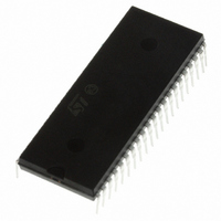
MCU 8BIT 32KB FLASH/ROM 42-SDIP
Manufacturer
STMicroelectronics
Series
ST7r
Datasheet
1.ST72F324BJ6B6.pdf
(193 pages)
Specifications of ST72F324BJ6B6
Core Processor
ST7
Core Size
8-Bit
Speed
8MHz
Connectivity
SCI, SPI
Peripherals
LVD, POR, PWM, WDT
Number Of I /o
32
Program Memory Size
32KB (32K x 8)
Program Memory Type
FLASH
Ram Size
1K x 8
Voltage - Supply (vcc/vdd)
3.8 V ~ 5.5 V
Data Converters
A/D 12x10b
Oscillator Type
Internal
Operating Temperature
-40°C ~ 85°C
Package / Case
42-SDIP (0.600", 15.24mm)
Controller Family/series
ST7
No. Of I/o's
32
Ram Memory Size
1KB
Cpu Speed
8MHz
No. Of Timers
2
Embedded Interface Type
SCI, SPI
No. Of Pwm Channels
3
Processor Series
ST72F3x
Core
ST7
Data Bus Width
8 bit
Data Ram Size
1 KB
Interface Type
SCI, SPI
Maximum Clock Frequency
8 MHz
Number Of Programmable I/os
32
Number Of Timers
3
Maximum Operating Temperature
+ 85 C
Mounting Style
Through Hole
Development Tools By Supplier
ST7232X-EVAL, ST7MDT20-DVP3, ST7MDT20J-EMU3, STX-RLINK
Minimum Operating Temperature
- 40 C
On-chip Adc
10 bit, 12 Channel
For Use With
497-6421 - BOARD EVAL DGTL BATT CHGR DESIGN497-5046 - KIT TOOL FOR ST7/UPSD/STR7 MCU
Lead Free Status / RoHS Status
Lead free / RoHS Compliant
Eeprom Size
-
Lead Free Status / Rohs Status
Details
Other names
497-5589-5


ST72324Bxx
12.5.2
Table 90.
1. Data based on characterization results, tested in production at V
2. Measurements are done in the following conditions:
3. All I/O pins in push-pull 0 mode (when applicable) with a static value at V
4. Data based on characterization results, not tested in production. All I/O pins in push-pull 0 mode (when applicable) with a
Symbol
I
- Program executed from RAM, CPU running with RAM access. The increase in consumption when executing from Flash is
50%.
- All I/O pins in input mode with a static value at V
- All peripherals in reset state
- LVD disabled
- Clock input (OSC1) driven by external square wave
- In Slow and Slow Wait modes, f
- To obtain the total current consumption of the device, add the clock source
consumption
characterization results, tested in production at V
static value at V
current consumption of the device, add the clock source consumption
DD
Supply current in Run mode
Supply current in Slow
mode
Supply current in Wait mode
Supply current in Slow Wait
mode
Supply current in Halt mode
Supply current in Active-halt
mode
Flash current consumption
Flash current consumption
(Section
(2)
(2)
(4)
DD
Parameter
or V
12.5.4).
SS
(no load); clock input (OSC1) driven by external square wave, LVD disabled. To obtain the total
CPU
is based on f
(3)
(2)
(2)
f
f
f
f
f
f
f
f
f
f
f
f
f
f
f
f
-40°C < T
-40°C < T
f
f
f
f
OSC
OSC
OSC
OSC
OSC
OSC
OSC
OSC
OSC
OSC
OSC
OSC
OSC
OSC
OSC
OSC
OSC
OSC
OSC
OSC
DD
DD
= 2 MHz, f
= 4 MHz, f
= 8 MHz, f
= 16 MHz, f
= 2 MHz, f
= 4 MHz, f
= 8 MHz, f
= 16 MHz, f
= 2 MHz, f
= 4 MHz, f
= 8 MHz, f
= 16 MHz, f
= 2 MHz, f
= 4 MHz, f
= 8 MHz, f
= 16 MHz, f
= 2 MHz
= 4 MHz
= 8 MHz
= 16 MHz
OSC
max. and f
or V
A
A
divided by 32
Conditions
< +85°C
< +125°C
SS
(no load)
CPU
CPU
CPU
CPU
CPU
CPU
CPU
CPU
CPU
CPU
CPU
CPU
CPU
CPU
CPU
CPU
CPU
DD
= 1 MHz
= 2 MHz
= 4 MHz
= 62.5 kHz
= 125 kHz
= 250 kHz
= 1 MHz
= 2 MHz
= 4 MHz
= 62.5 kHz
= 125 kHz
= 250 kHz
max.
max. and f
= 8 MHz
= 500 kHz
= 8 MHz
= 500 kHz
(Section
DD
or V
(Section
CPU
12.6.3).
SS
1050
Typ
(no load), LVD disabled. Data based on
580
650
770
365
380
410
500
max.
1.3
2.0
3.6
7.1
0.6
0.7
0.8
1.1
0.8
1.2
2.0
3.5
<1
5
32 Kbyte
12.6.3) and the peripheral power
Flash
Max
1200
1300
1800
2000
15.0
475
500
550
650
3.0
5.0
8.0
2.7
3.0
3.6
4.0
3.0
4.0
5.0
7.0
10
50
Electrical characteristics
(1)
0.48
0.53
0.63
0.80
Typ
430
470
530
660
315
330
360
460
1.4
2.4
4.4
0.6
0.9
1.3
2.3
<1
<1
16/8 Kbyte
1
Flash
Max
1000
1050
1200
950
425
450
500
600
2.3
3.5
5.3
7.0
1.1
1.2
1.4
1.8
2.2
2.6
3.6
10
50
1
(1)
147/193
Unit
mA
µA
Related parts for ST72F324BJ6B6
Image
Part Number
Description
Manufacturer
Datasheet
Request
R

Part Number:
Description:
STMicroelectronics [RIPPLE-CARRY BINARY COUNTER/DIVIDERS]
Manufacturer:
STMicroelectronics
Datasheet:
Part Number:
Description:
STMicroelectronics [LIQUID-CRYSTAL DISPLAY DRIVERS]
Manufacturer:
STMicroelectronics
Datasheet:

Part Number:
Description:
BOARD EVAL FOR MEMS SENSORS
Manufacturer:
STMicroelectronics
Datasheet:
Part Number:
Description:
NPN TRANSISTOR POWER MODULE
Manufacturer:
STMicroelectronics
Datasheet:
Part Number:
Description:
TURBOSWITCH ULTRA-FAST HIGH VOLTAGE DIODE
Manufacturer:
STMicroelectronics
Datasheet:
Part Number:
Description:
Manufacturer:
STMicroelectronics
Datasheet:
Part Number:
Description:
DIODE / SCR MODULE
Manufacturer:
STMicroelectronics
Datasheet:
Part Number:
Description:
DIODE / SCR MODULE
Manufacturer:
STMicroelectronics
Datasheet:
Part Number:
Description:
Search -----> STE16N100
Manufacturer:
STMicroelectronics
Datasheet:
Part Number:
Description:
Search ---> STE53NA50
Manufacturer:
STMicroelectronics
Datasheet:
Part Number:
Description:
NPN Transistor Power Module
Manufacturer:
STMicroelectronics
Datasheet: