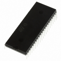
ST72F324BJ6B6 STMicroelectronics, ST72F324BJ6B6 Datasheet - Page 37

ST72F324BJ6B6
Manufacturer Part Number
ST72F324BJ6B6
Description
MCU 8BIT 32KB FLASH/ROM 42-SDIP
Manufacturer
STMicroelectronics
Series
ST7r
Datasheet
1.ST72F324BJ6B6.pdf
(193 pages)
Specifications of ST72F324BJ6B6
Core Processor
ST7
Core Size
8-Bit
Speed
8MHz
Connectivity
SCI, SPI
Peripherals
LVD, POR, PWM, WDT
Number Of I /o
32
Program Memory Size
32KB (32K x 8)
Program Memory Type
FLASH
Ram Size
1K x 8
Voltage - Supply (vcc/vdd)
3.8 V ~ 5.5 V
Data Converters
A/D 12x10b
Oscillator Type
Internal
Operating Temperature
-40°C ~ 85°C
Package / Case
42-SDIP (0.600", 15.24mm)
Controller Family/series
ST7
No. Of I/o's
32
Ram Memory Size
1KB
Cpu Speed
8MHz
No. Of Timers
2
Embedded Interface Type
SCI, SPI
No. Of Pwm Channels
3
Processor Series
ST72F3x
Core
ST7
Data Bus Width
8 bit
Data Ram Size
1 KB
Interface Type
SCI, SPI
Maximum Clock Frequency
8 MHz
Number Of Programmable I/os
32
Number Of Timers
3
Maximum Operating Temperature
+ 85 C
Mounting Style
Through Hole
Development Tools By Supplier
ST7232X-EVAL, ST7MDT20-DVP3, ST7MDT20J-EMU3, STX-RLINK
Minimum Operating Temperature
- 40 C
On-chip Adc
10 bit, 12 Channel
For Use With
497-6421 - BOARD EVAL DGTL BATT CHGR DESIGN497-5046 - KIT TOOL FOR ST7/UPSD/STR7 MCU
Lead Free Status / RoHS Status
Lead free / RoHS Compliant
Eeprom Size
-
Lead Free Status / Rohs Status
Details
Other names
497-5589-5
- Current page: 37 of 193
- Download datasheet (3Mb)
ST72324Bxx
Note:
6.5.2
Caution:
1
2
3
4
Provided the minimum V
MCU can only be in two modes:
In these conditions, secure operation is always ensured for the application without the need
for external reset hardware.
During an LVD reset, the RESET pin is held low, thus permitting the MCU to reset other
devices.
The LVD allows the device to be used without any external reset circuitry.
If the medium or low thresholds are selected, the detection may occur outside the specified
operating voltage range. Below 3.8 V, device operation is not guaranteed.
The LVD is an optional function which can be selected by option byte.
It is recommended to make sure that the V
device is exiting from reset, to ensure the application functions properly.
Figure 16. Low voltage detector vs reset
AVD (auxiliary voltage detector)
The AVD is based on an analog comparison between a V
value and the V
V
The output of the AVD comparator is directly readable by the application software through a
real-time status bit (AVDF) in the SICSR register. This bit is read only.
The AVD function is active only if the LVD is enabled through the option byte (see
Section 14.1 on page
Monitoring the V
The AVD voltage threshold value is relative to the selected LVD threshold configured by
option byte (see
If the AVD interrupt is enabled, an interrupt is generated when the voltage crosses the
V
In the case of a drop in voltage, the AVD interrupt acts as an early warning, allowing
software to shut down safely before the LVD resets the microcontroller. See
IT+
IT+(AVD)
reference value for rising voltage in order to avoid parasitic detection (hysteresis).
–
–
RESET
under full software control
in static safe reset
or V
V
V
IT-
IT+
IT-(AVD)
V
DD
DD
Section 14.1 on page
main supply. The V
DD
threshold (AVDF bit toggles).
179).
main supply
DD
value (guaranteed for the oscillator frequency) is above V
IT-
179).
reference value for falling voltage is lower than the
DD
supply voltage rises monotonously when the
V
hys
Supply, reset and clock management
IT-(AVD)
and V
IT+(AVD)
Figure
reference
17.
IT-
37/193
, the
Related parts for ST72F324BJ6B6
Image
Part Number
Description
Manufacturer
Datasheet
Request
R

Part Number:
Description:
STMicroelectronics [RIPPLE-CARRY BINARY COUNTER/DIVIDERS]
Manufacturer:
STMicroelectronics
Datasheet:

Part Number:
Description:
STMicroelectronics [LIQUID-CRYSTAL DISPLAY DRIVERS]
Manufacturer:
STMicroelectronics
Datasheet:

Part Number:
Description:
BOARD EVAL FOR MEMS SENSORS
Manufacturer:
STMicroelectronics
Datasheet:

Part Number:
Description:
NPN TRANSISTOR POWER MODULE
Manufacturer:
STMicroelectronics
Datasheet:

Part Number:
Description:
TURBOSWITCH ULTRA-FAST HIGH VOLTAGE DIODE
Manufacturer:
STMicroelectronics
Datasheet:

Part Number:
Description:
Manufacturer:
STMicroelectronics
Datasheet:

Part Number:
Description:
DIODE / SCR MODULE
Manufacturer:
STMicroelectronics
Datasheet:

Part Number:
Description:
DIODE / SCR MODULE
Manufacturer:
STMicroelectronics
Datasheet:

Part Number:
Description:
Search -----> STE16N100
Manufacturer:
STMicroelectronics
Datasheet:

Part Number:
Description:
Search ---> STE53NA50
Manufacturer:
STMicroelectronics
Datasheet:

Part Number:
Description:
NPN Transistor Power Module
Manufacturer:
STMicroelectronics
Datasheet:


