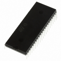
ST72F324BJ6B6 STMicroelectronics, ST72F324BJ6B6 Datasheet - Page 189

ST72F324BJ6B6
Manufacturer Part Number
ST72F324BJ6B6
Description
MCU 8BIT 32KB FLASH/ROM 42-SDIP
Manufacturer
STMicroelectronics
Series
ST7r
Datasheet
1.ST72F324BJ6B6.pdf
(193 pages)
Specifications of ST72F324BJ6B6
Core Processor
ST7
Core Size
8-Bit
Speed
8MHz
Connectivity
SCI, SPI
Peripherals
LVD, POR, PWM, WDT
Number Of I /o
32
Program Memory Size
32KB (32K x 8)
Program Memory Type
FLASH
Ram Size
1K x 8
Voltage - Supply (vcc/vdd)
3.8 V ~ 5.5 V
Data Converters
A/D 12x10b
Oscillator Type
Internal
Operating Temperature
-40°C ~ 85°C
Package / Case
42-SDIP (0.600", 15.24mm)
Controller Family/series
ST7
No. Of I/o's
32
Ram Memory Size
1KB
Cpu Speed
8MHz
No. Of Timers
2
Embedded Interface Type
SCI, SPI
No. Of Pwm Channels
3
Processor Series
ST72F3x
Core
ST7
Data Bus Width
8 bit
Data Ram Size
1 KB
Interface Type
SCI, SPI
Maximum Clock Frequency
8 MHz
Number Of Programmable I/os
32
Number Of Timers
3
Maximum Operating Temperature
+ 85 C
Mounting Style
Through Hole
Development Tools By Supplier
ST7232X-EVAL, ST7MDT20-DVP3, ST7MDT20J-EMU3, STX-RLINK
Minimum Operating Temperature
- 40 C
On-chip Adc
10 bit, 12 Channel
For Use With
497-6421 - BOARD EVAL DGTL BATT CHGR DESIGN497-5046 - KIT TOOL FOR ST7/UPSD/STR7 MCU
Lead Free Status / RoHS Status
Lead free / RoHS Compliant
Eeprom Size
-
Lead Free Status / Rohs Status
Details
Other names
497-5589-5
- Current page: 189 of 193
- Download datasheet (3Mb)
ST72324Bxx
15.2
15.2.1
15.2.2
15.3
15.3.1
15.3.2
In the same way, as long as the SBK bit is set, break characters are sent to the TDO pin.
This may lead to generate one break more than expected.
Occurrence
The occurrence of the problem is random and proportional to the baud rate. With a transmit
frequency of 19200 baud (f
occurrence is around 1%.
Workaround
If this wrong duration is not compliant with the communication protocol in the application,
software can request that an Idle line be generated before the break character. In this case,
the break duration is always correct assuming the application is not doing anything between
the idle and the break. This can be ensured by temporarily disabling interrupts.
The exact sequence is:
1.
2.
3.
4.
8/16 Kbyte Flash devices only
39-pulse ICC entry mode
ICC mode entry using ST7 application clock (39 pulses) is not supported. External clock
mode must be used (36 pulses). Refer to the ST7 Flash Programming Reference Manual.
Negative current injection on pin PB0
Negative current injection on pin PB0 degrades the performance of the device and is not
allowed on this pin.
8/16 Kbyte ROM devices only
Readout protection with LVD
Readout protection is not supported if the LVD is enabled.
I/O Port A and F configuration
When using an external quartz crystal or ceramic resonator, a few f
be lost when the signal pattern in
device to enter test mode and return to user mode after a few clock periods. User program
execution and I/O status are not changed, only a few clock cycles are lost.
This happens with either one of the following configurations
●
●
This is detailed in
Disable interrupts
Reset and set TE (IDLE request)
Set and reset SBK (break request)
Re-enable interrupts
PA3 = 0, PF4 = 1, PF1 = 0 while PLL option is disabled and PF0 is toggling
PA3 = 0, PF4 = 1, PF1 = 0, PF0 = 1 while PLL option is enabled
Table
125.
CPU
= 8MHz and SCIBRR = 0xC9), the wrong break duration
Table 125
occurs. This is because this pattern causes the
OSC2
Known limitations
clock periods may
189/193
Related parts for ST72F324BJ6B6
Image
Part Number
Description
Manufacturer
Datasheet
Request
R

Part Number:
Description:
STMicroelectronics [RIPPLE-CARRY BINARY COUNTER/DIVIDERS]
Manufacturer:
STMicroelectronics
Datasheet:

Part Number:
Description:
STMicroelectronics [LIQUID-CRYSTAL DISPLAY DRIVERS]
Manufacturer:
STMicroelectronics
Datasheet:

Part Number:
Description:
BOARD EVAL FOR MEMS SENSORS
Manufacturer:
STMicroelectronics
Datasheet:

Part Number:
Description:
NPN TRANSISTOR POWER MODULE
Manufacturer:
STMicroelectronics
Datasheet:

Part Number:
Description:
TURBOSWITCH ULTRA-FAST HIGH VOLTAGE DIODE
Manufacturer:
STMicroelectronics
Datasheet:

Part Number:
Description:
Manufacturer:
STMicroelectronics
Datasheet:

Part Number:
Description:
DIODE / SCR MODULE
Manufacturer:
STMicroelectronics
Datasheet:

Part Number:
Description:
DIODE / SCR MODULE
Manufacturer:
STMicroelectronics
Datasheet:

Part Number:
Description:
Search -----> STE16N100
Manufacturer:
STMicroelectronics
Datasheet:

Part Number:
Description:
Search ---> STE53NA50
Manufacturer:
STMicroelectronics
Datasheet:

Part Number:
Description:
NPN Transistor Power Module
Manufacturer:
STMicroelectronics
Datasheet:


