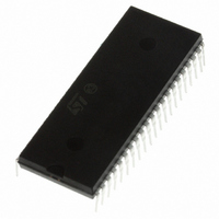
ST72F324BJ6B6 STMicroelectronics, ST72F324BJ6B6 Datasheet - Page 158

ST72F324BJ6B6
Manufacturer Part Number
ST72F324BJ6B6
Description
MCU 8BIT 32KB FLASH/ROM 42-SDIP
Manufacturer
STMicroelectronics
Series
ST7r
Datasheet
1.ST72F324BJ6B6.pdf
(193 pages)
Specifications of ST72F324BJ6B6
Core Processor
ST7
Core Size
8-Bit
Speed
8MHz
Connectivity
SCI, SPI
Peripherals
LVD, POR, PWM, WDT
Number Of I /o
32
Program Memory Size
32KB (32K x 8)
Program Memory Type
FLASH
Ram Size
1K x 8
Voltage - Supply (vcc/vdd)
3.8 V ~ 5.5 V
Data Converters
A/D 12x10b
Oscillator Type
Internal
Operating Temperature
-40°C ~ 85°C
Package / Case
42-SDIP (0.600", 15.24mm)
Controller Family/series
ST7
No. Of I/o's
32
Ram Memory Size
1KB
Cpu Speed
8MHz
No. Of Timers
2
Embedded Interface Type
SCI, SPI
No. Of Pwm Channels
3
Processor Series
ST72F3x
Core
ST7
Data Bus Width
8 bit
Data Ram Size
1 KB
Interface Type
SCI, SPI
Maximum Clock Frequency
8 MHz
Number Of Programmable I/os
32
Number Of Timers
3
Maximum Operating Temperature
+ 85 C
Mounting Style
Through Hole
Development Tools By Supplier
ST7232X-EVAL, ST7MDT20-DVP3, ST7MDT20J-EMU3, STX-RLINK
Minimum Operating Temperature
- 40 C
On-chip Adc
10 bit, 12 Channel
For Use With
497-6421 - BOARD EVAL DGTL BATT CHGR DESIGN497-5046 - KIT TOOL FOR ST7/UPSD/STR7 MCU
Lead Free Status / RoHS Status
Lead free / RoHS Compliant
Eeprom Size
-
Lead Free Status / Rohs Status
Details
Other names
497-5589-5
- Current page: 158 of 193
- Download datasheet (3Mb)
Electrical characteristics
12.9
12.9.1
Table 106. General characteristics
1. Data based on characterization results, not tested in production.
2. Hysteresis voltage between Schmitt trigger switching levels. Based on characterization results, not tested.
3. When the current limitation is not possible, the V
4. No negative current injection allowed on 8/16 Kbyte Flash devices
5. Static peak current value taken at a fixed V
6. The Schmitt trigger that is connected to every I/O port is disabled for analog inputs only when ADON bit is ON and the
7. The R
8. To generate an external interrupt, a minimum pulse width has to be applied on an I/O port pin configured as an external
158/193
ΣI
I
INJ(PIN)
Symbol
INJ(PIN)
t
t
t
f(IO)out
r(IO)out
specification. A positive injection is induced by V
Section 12.2.2 on page 143
in production. This value depends on V
particular ADC channel is selected (with port configured in input floating mode). When the ADON bit is OFF, static current
consumption may result. This can be avoided by keeping the input voltage of this pin close to V
Figure
interrupt source.
w(IT)in
V
R
C
V
V
I
I
lkg
hys
PU
S
IH
IO
IL
PU
(3)
(3)
71).
pull-up equivalent resistor is based on a resistive transistor (corresponding I
Input low level voltage
(standard voltage devices)
Input high level voltage
Schmitt trigger voltage hysteresis
Injected current on I/O pins other than
pin PB0
Injected current on ROM and 32 Kbyte
Flash devices pin PB0
Injected current on 8/16 Kbyte Flash
devices pin PB0
Total injected current
(sum of all I/O and control pins)
Input leakage current
Static current consumption induced by
each floating input pin
Weak pull-up equivalent resistor
I/O pin capacitance
Output high to low level fall time
Output low to high level rise time
External interrupt pulse time
I/O port pin characteristics
General characteristics
Subject to general operating conditions for V
(4)
Parameter
for more details.
(1)
DD
(1)
and temperature values.
(8)
IN
value, based on design simulation and technology characteristics, not tested
(1)
(7)
(1)
(2)
IN
IN
maximum must be respected, otherwise refer to the I
> V
DD
while a negative injection is induced by V
V
V
V
Floating input mode
V
C
between 10% and 90%
DD
DD
SS
IN
L
= 50 pF
=
<
= 5 V
= 5 V
V
Conditions
V
SS,
IN
DD
<
V
, f
V
DD
OSC
DD
= 5 V
, and T
(5)(6)
PU
A
current characteristics described in
0.7xV
unless otherwise specified.
Min
50
0
1
DD
DD
or V
IN
Typ
200
120
0.7
< V
25
25
5
SS
INJ(PIN)
SS
.
. Refer to
0.3xV
ST72324Bxx
Max
±25
250
±4
+4
±1
DD
t
Unit
mA
mA
CPU
µA
kΩ
pF
ns
V
Related parts for ST72F324BJ6B6
Image
Part Number
Description
Manufacturer
Datasheet
Request
R

Part Number:
Description:
STMicroelectronics [RIPPLE-CARRY BINARY COUNTER/DIVIDERS]
Manufacturer:
STMicroelectronics
Datasheet:

Part Number:
Description:
STMicroelectronics [LIQUID-CRYSTAL DISPLAY DRIVERS]
Manufacturer:
STMicroelectronics
Datasheet:

Part Number:
Description:
BOARD EVAL FOR MEMS SENSORS
Manufacturer:
STMicroelectronics
Datasheet:

Part Number:
Description:
NPN TRANSISTOR POWER MODULE
Manufacturer:
STMicroelectronics
Datasheet:

Part Number:
Description:
TURBOSWITCH ULTRA-FAST HIGH VOLTAGE DIODE
Manufacturer:
STMicroelectronics
Datasheet:

Part Number:
Description:
Manufacturer:
STMicroelectronics
Datasheet:

Part Number:
Description:
DIODE / SCR MODULE
Manufacturer:
STMicroelectronics
Datasheet:

Part Number:
Description:
DIODE / SCR MODULE
Manufacturer:
STMicroelectronics
Datasheet:

Part Number:
Description:
Search -----> STE16N100
Manufacturer:
STMicroelectronics
Datasheet:

Part Number:
Description:
Search ---> STE53NA50
Manufacturer:
STMicroelectronics
Datasheet:

Part Number:
Description:
NPN Transistor Power Module
Manufacturer:
STMicroelectronics
Datasheet:


