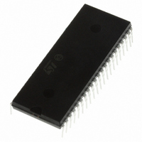
ST72F324BJ6B6 STMicroelectronics, ST72F324BJ6B6 Datasheet - Page 159

ST72F324BJ6B6
Manufacturer Part Number
ST72F324BJ6B6
Description
MCU 8BIT 32KB FLASH/ROM 42-SDIP
Manufacturer
STMicroelectronics
Series
ST7r
Datasheet
1.ST72F324BJ6B6.pdf
(193 pages)
Specifications of ST72F324BJ6B6
Core Processor
ST7
Core Size
8-Bit
Speed
8MHz
Connectivity
SCI, SPI
Peripherals
LVD, POR, PWM, WDT
Number Of I /o
32
Program Memory Size
32KB (32K x 8)
Program Memory Type
FLASH
Ram Size
1K x 8
Voltage - Supply (vcc/vdd)
3.8 V ~ 5.5 V
Data Converters
A/D 12x10b
Oscillator Type
Internal
Operating Temperature
-40°C ~ 85°C
Package / Case
42-SDIP (0.600", 15.24mm)
Controller Family/series
ST7
No. Of I/o's
32
Ram Memory Size
1KB
Cpu Speed
8MHz
No. Of Timers
2
Embedded Interface Type
SCI, SPI
No. Of Pwm Channels
3
Processor Series
ST72F3x
Core
ST7
Data Bus Width
8 bit
Data Ram Size
1 KB
Interface Type
SCI, SPI
Maximum Clock Frequency
8 MHz
Number Of Programmable I/os
32
Number Of Timers
3
Maximum Operating Temperature
+ 85 C
Mounting Style
Through Hole
Development Tools By Supplier
ST7232X-EVAL, ST7MDT20-DVP3, ST7MDT20J-EMU3, STX-RLINK
Minimum Operating Temperature
- 40 C
On-chip Adc
10 bit, 12 Channel
For Use With
497-6421 - BOARD EVAL DGTL BATT CHGR DESIGN497-5046 - KIT TOOL FOR ST7/UPSD/STR7 MCU
Lead Free Status / RoHS Status
Lead free / RoHS Compliant
Eeprom Size
-
Lead Free Status / Rohs Status
Details
Other names
497-5589-5
- Current page: 159 of 193
- Download datasheet (3Mb)
ST72324Bxx
12.9.2
Table 107. Output driving current
1. The I
2. The I
Symbol
V
V
OH
ports and control pins) must not exceed I
(I/O ports and control pins) must not exceed I
OL
(1)
(2)
IO
IO
current sunk must always respect the absolute maximum rating specified in
current sourced must always respect the absolute maximum rating specified in
Output low level voltage for a standard I/O
pin when 8 pins are sunk at same time
(see
Output low level voltage for a high sink I/O
pin when 4 pins are sunk at same time
(see
Output high level voltage for an I/O pin
when 4 pins are sourced at same time
(see
Figure 70. Unused I/O pins configured as input
1. I/O can be left unconnected if it is configured as output (0 or 1) by the software. This has the advantage of
Figure 71. Typical I
Output driving current
Subject to general operating conditions for V
Figure
Figure 73
Figure 74
greater EMC robustness and lower cost.
72)
and
and
Parameter
Figure
Figure
75)
77)
PU
VSS
vs. V
.
VDD
. True open drain I/O pins do not have V
DD
with V
90
80
70
60
50
40
30
20
10
V
0
DD
2
10 kΩ
10 kΩ
2.5
V
DD
IN
Ta=1 40°C
Ta=9 5°C
Ta=2 5°C
Ta=-45 °C
3
= V
= 5V
Unused I/O port
3.5
Unused I/O port
DD
Conditions
Vdd(V)
SS
4
, f
4.5
CPU
ST7XXX
ST7XXX
I
I
I
T
T
I
I
T
T
I
IO
IO
IO
IO
IO
IO
A
A
A
A
(1)
5
= +5 mA
= +2 mA
= +20 mA
< 85 °C
> 85 °C
= +8 mA
= -5 mA,
< 85 °C
> 85 °C
= -2 mA
, and T
5.5
Section 12.2.2
6
A
Section 12.2.2
unless otherwise specified.
OH
.
Electrical characteristics
V
V
V
DD
DD
DD
Min
and the sum of I
- 1.4
- 1.6
- 0.7
and the sum of I
Max
1.2
0.5
1.3
1.5
0.6
IO
159/193
(I/O
IO
Unit
V
Related parts for ST72F324BJ6B6
Image
Part Number
Description
Manufacturer
Datasheet
Request
R

Part Number:
Description:
STMicroelectronics [RIPPLE-CARRY BINARY COUNTER/DIVIDERS]
Manufacturer:
STMicroelectronics
Datasheet:

Part Number:
Description:
STMicroelectronics [LIQUID-CRYSTAL DISPLAY DRIVERS]
Manufacturer:
STMicroelectronics
Datasheet:

Part Number:
Description:
BOARD EVAL FOR MEMS SENSORS
Manufacturer:
STMicroelectronics
Datasheet:

Part Number:
Description:
NPN TRANSISTOR POWER MODULE
Manufacturer:
STMicroelectronics
Datasheet:

Part Number:
Description:
TURBOSWITCH ULTRA-FAST HIGH VOLTAGE DIODE
Manufacturer:
STMicroelectronics
Datasheet:

Part Number:
Description:
Manufacturer:
STMicroelectronics
Datasheet:

Part Number:
Description:
DIODE / SCR MODULE
Manufacturer:
STMicroelectronics
Datasheet:

Part Number:
Description:
DIODE / SCR MODULE
Manufacturer:
STMicroelectronics
Datasheet:

Part Number:
Description:
Search -----> STE16N100
Manufacturer:
STMicroelectronics
Datasheet:

Part Number:
Description:
Search ---> STE53NA50
Manufacturer:
STMicroelectronics
Datasheet:

Part Number:
Description:
NPN Transistor Power Module
Manufacturer:
STMicroelectronics
Datasheet:


