MC9S12NE64VTU Freescale Semiconductor, MC9S12NE64VTU Datasheet - Page 276
MC9S12NE64VTU
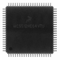
Manufacturer Part Number
MC9S12NE64VTU
Description
IC MCU 25MHZ ETHERNET/PHY 80TQFP
Manufacturer
Freescale Semiconductor
Series
HCS12r
Datasheet
1.MC9S12NE64VTU.pdf
(554 pages)
Specifications of MC9S12NE64VTU
Mfg Application Notes
MC9S12NE64 Integrated Ethernet Controller Implementing an Ethernet Interface with the MC9S12NE64 Web Server Development with MC9S12NE64 and Open TCP
Core Processor
HCS12
Core Size
16-Bit
Speed
25MHz
Connectivity
EBI/EMI, Ethernet, I²C, SCI, SPI
Peripherals
POR, PWM, WDT
Number Of I /o
38
Program Memory Size
64KB (64K x 8)
Program Memory Type
FLASH
Ram Size
8K x 8
Voltage - Supply (vcc/vdd)
2.375 V ~ 3.465 V
Data Converters
A/D 8x10b
Oscillator Type
Internal
Operating Temperature
-40°C ~ 105°C
Package / Case
80-TQFP Exposed Pad, 80-eTQFP, 80-HTQFP, 80-VQFP
Data Bus Width
16 bit
Data Ram Size
8 KB
Interface Type
I2C, SCI, SPI
Maximum Clock Frequency
25 MHz
Number Of Programmable I/os
70
Number Of Timers
16 bit
Operating Supply Voltage
- 0.3 V to + 3 V
Maximum Operating Temperature
+ 105 C
Mounting Style
SMD/SMT
Minimum Operating Temperature
- 65 C
On-chip Adc
10 bit
For Use With
EVB9S12NE64E - BOARD EVAL FOR 9S12NE64DEMO9S12NE64E - DEMO BOARD FOR 9S12NE64
Lead Free Status / RoHS Status
Lead free / RoHS Compliant
Eeprom Size
-
Lead Free Status / Rohs Status
Details
Available stocks
Company
Part Number
Manufacturer
Quantity
Price
Company:

Part Number:
MC9S12NE64VTU
Manufacturer:
FREESCALE
Quantity:
1 831
Company:
Part Number:
MC9S12NE64VTU
Manufacturer:
Freescale Semiconductor
Quantity:
10 000
Company:
Part Number:
MC9S12NE64VTUE
Manufacturer:
Freescale Semiconductor
Quantity:
10 000
Part Number:
MC9S12NE64VTUE
Manufacturer:
FREESCALE
Quantity:
20 000


Chapter 9 Serial Peripheral Interface (SPIV3)
In master mode, with slave select output enabled the SS line is always deasserted and reasserted between
successive transfers for at least minimum idle time.
9.4.3.3
Some peripherals require the first SCK edge before the first data bit becomes available at the data out pin,
the second edge clocks data into the system. In this format, the first SCK edge is issued by setting the
CPHA bit at the beginning of the 8-cycle transfer operation.
The first edge of SCK occurs immediately after the half SCK clock cycle synchronization delay. This first
edge commands the slave to transfer its first data bit to the serial data input pin of the master.
A half SCK cycle later, the second edge appears on the SCK pin. This is the latching edge for both the
master and slave.
When the third edge occurs, the value previously latched from the serial data input pin is shifted into the
LSB or MSB of the SPI shift register, depending on LSBFE bit. After this edge, the next bit of the master
data is coupled out of the serial data output pin of the master to the serial input pin on the slave.
This process continues for a total of 16 edges on the SCK line with data being latched on even numbered
edges and shifting taking place on odd numbered edges.
Data reception is double buffered, data is serially shifted into the SPI shift register during the transfer and
is transferred to the parallel SPI Data Register after the last bit is shifted in.
After the 16th SCK edge:
Figure 9-10
slave timing diagram because the SCK, MISO, and MOSI pins are connected directly between the master
and the slave. The MISO signal is the output from the slave, and the MOSI signal is the output from the
master. The SS line is the slave select input to the slave. The SS pin of the master must be either high or
reconfigured as a general-purpose output not affecting the SPI.
The SS line can remain active low between successive transfers (can be tied low at all times). This format
is sometimes preferred in systems having a single fixed master and a single slave that drive the MISO data
line.
In master mode, if a transmission has completed and a new data byte is available in the SPI Data Register,
this byte is send out immediately without a trailing and minimum idle time.
The SPI interrupt request flag (SPIF) is common to both the master and slave modes. SPIF gets set one
half SCK cycle after the last SCK edge.
276
•
•
•
Data that was previously in the SPI Data Register of the master is now in the data register of the
slave, and data that was in the data register of the slave is in the master.
The SPIF flag bit in SPISR is set indicating that the transfer is complete.
Back-to-back transfers in master mode
shows two clocking variations for CPHA = 1. The diagram may be interpreted as a master or
CPHA = 1 Transfer Format
MC9S12NE64 Data Sheet, Rev. 1.1
Freescale Semiconductor
Related parts for MC9S12NE64VTU
Image
Part Number
Description
Manufacturer
Datasheet
Request
R

Part Number:
Description:
Manufacturer:
Freescale Semiconductor, Inc
Datasheet:
Part Number:
Description:
Manufacturer:
Freescale Semiconductor, Inc
Datasheet:
Part Number:
Description:
Manufacturer:
Freescale Semiconductor, Inc
Datasheet:
Part Number:
Description:
Manufacturer:
Freescale Semiconductor, Inc
Datasheet:
Part Number:
Description:
Manufacturer:
Freescale Semiconductor, Inc
Datasheet:
Part Number:
Description:
Manufacturer:
Freescale Semiconductor, Inc
Datasheet:
Part Number:
Description:
Manufacturer:
Freescale Semiconductor, Inc
Datasheet:
Part Number:
Description:
Manufacturer:
Freescale Semiconductor, Inc
Datasheet:
Part Number:
Description:
Manufacturer:
Freescale Semiconductor, Inc
Datasheet:
Part Number:
Description:
Manufacturer:
Freescale Semiconductor, Inc
Datasheet:
Part Number:
Description:
Manufacturer:
Freescale Semiconductor, Inc
Datasheet:
Part Number:
Description:
Manufacturer:
Freescale Semiconductor, Inc
Datasheet:
Part Number:
Description:
Manufacturer:
Freescale Semiconductor, Inc
Datasheet:
Part Number:
Description:
Manufacturer:
Freescale Semiconductor, Inc
Datasheet:
Part Number:
Description:
Manufacturer:
Freescale Semiconductor, Inc
Datasheet: