MC9S12NE64VTU Freescale Semiconductor, MC9S12NE64VTU Datasheet - Page 403
MC9S12NE64VTU
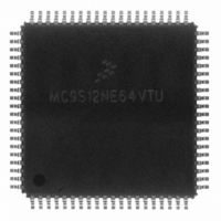
Manufacturer Part Number
MC9S12NE64VTU
Description
IC MCU 25MHZ ETHERNET/PHY 80TQFP
Manufacturer
Freescale Semiconductor
Series
HCS12r
Datasheet
1.MC9S12NE64VTU.pdf
(554 pages)
Specifications of MC9S12NE64VTU
Mfg Application Notes
MC9S12NE64 Integrated Ethernet Controller Implementing an Ethernet Interface with the MC9S12NE64 Web Server Development with MC9S12NE64 and Open TCP
Core Processor
HCS12
Core Size
16-Bit
Speed
25MHz
Connectivity
EBI/EMI, Ethernet, I²C, SCI, SPI
Peripherals
POR, PWM, WDT
Number Of I /o
38
Program Memory Size
64KB (64K x 8)
Program Memory Type
FLASH
Ram Size
8K x 8
Voltage - Supply (vcc/vdd)
2.375 V ~ 3.465 V
Data Converters
A/D 8x10b
Oscillator Type
Internal
Operating Temperature
-40°C ~ 105°C
Package / Case
80-TQFP Exposed Pad, 80-eTQFP, 80-HTQFP, 80-VQFP
Data Bus Width
16 bit
Data Ram Size
8 KB
Interface Type
I2C, SCI, SPI
Maximum Clock Frequency
25 MHz
Number Of Programmable I/os
70
Number Of Timers
16 bit
Operating Supply Voltage
- 0.3 V to + 3 V
Maximum Operating Temperature
+ 105 C
Mounting Style
SMD/SMT
Minimum Operating Temperature
- 65 C
On-chip Adc
10 bit
For Use With
EVB9S12NE64E - BOARD EVAL FOR 9S12NE64DEMO9S12NE64E - DEMO BOARD FOR 9S12NE64
Lead Free Status / RoHS Status
Lead free / RoHS Compliant
Eeprom Size
-
Lead Free Status / Rohs Status
Details
Available stocks
Company
Part Number
Manufacturer
Quantity
Price
Company:

Part Number:
MC9S12NE64VTU
Manufacturer:
FREESCALE
Quantity:
1 831
Company:
Part Number:
MC9S12NE64VTU
Manufacturer:
Freescale Semiconductor
Quantity:
10 000
Company:
Part Number:
MC9S12NE64VTUE
Manufacturer:
Freescale Semiconductor
Quantity:
10 000
Part Number:
MC9S12NE64VTUE
Manufacturer:
FREESCALE
Quantity:
20 000


15.3.2.4
Read: Anytime when register is in the map
Write: Anytime when register is in the map
This register controls the data direction for port B. When port B is operating as a general-purpose I/O port,
DDRB determines the primary direction for each port B pin. A 1 causes the associated port pin to be an
output and a 0 causes the associated pin to be a high-impedance input. The value in a DDR bit also affects
the source of data for reads of the corresponding PORTB register. If the DDR bit is 0 (input) the buffered
pin input state is read. If the DDR bit is 1 (output) the associated port data register bit state is read.
This register is not in the on-chip memory map in expanded and special peripheral modes. Therefore, these
accesses will be echoed externally. It is reset to 0x00 so the DDR does not override the three-state control
signals.
Freescale Semiconductor
Reset
DDRB
Field
7:0
W
R
Bit 7
Data Direction Port B
0 Configure the corresponding I/O pin as an input
1 Configure the corresponding I/O pin as an output
Data Direction Register B (DDRB)
0
7
6
0
6
Figure 15-5. Data Direction Register B (DDRB)
Table 15-4. DDRB Field Descriptions
MC9S12NE64 Data Sheet, Rev. 1.1
5
0
5
4
0
4
Description
3
0
3
2
0
2
Memory Map and Register Definition
1
0
1
Bit 0
0
0
403
Related parts for MC9S12NE64VTU
Image
Part Number
Description
Manufacturer
Datasheet
Request
R

Part Number:
Description:
Manufacturer:
Freescale Semiconductor, Inc
Datasheet:
Part Number:
Description:
Manufacturer:
Freescale Semiconductor, Inc
Datasheet:
Part Number:
Description:
Manufacturer:
Freescale Semiconductor, Inc
Datasheet:
Part Number:
Description:
Manufacturer:
Freescale Semiconductor, Inc
Datasheet:
Part Number:
Description:
Manufacturer:
Freescale Semiconductor, Inc
Datasheet:
Part Number:
Description:
Manufacturer:
Freescale Semiconductor, Inc
Datasheet:
Part Number:
Description:
Manufacturer:
Freescale Semiconductor, Inc
Datasheet:
Part Number:
Description:
Manufacturer:
Freescale Semiconductor, Inc
Datasheet:
Part Number:
Description:
Manufacturer:
Freescale Semiconductor, Inc
Datasheet:
Part Number:
Description:
Manufacturer:
Freescale Semiconductor, Inc
Datasheet:
Part Number:
Description:
Manufacturer:
Freescale Semiconductor, Inc
Datasheet:
Part Number:
Description:
Manufacturer:
Freescale Semiconductor, Inc
Datasheet:
Part Number:
Description:
Manufacturer:
Freescale Semiconductor, Inc
Datasheet:
Part Number:
Description:
Manufacturer:
Freescale Semiconductor, Inc
Datasheet:
Part Number:
Description:
Manufacturer:
Freescale Semiconductor, Inc
Datasheet: