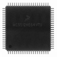
MC9S12NE64VTU Freescale Semiconductor, MC9S12NE64VTU Datasheet - Page 383

MC9S12NE64VTU
Manufacturer Part Number
MC9S12NE64VTU
Description
IC MCU 25MHZ ETHERNET/PHY 80TQFP
Manufacturer
Freescale Semiconductor
Series
HCS12r
Datasheet
1.MC9S12NE64VTU.pdf
(554 pages)
Specifications of MC9S12NE64VTU
Mfg Application Notes
MC9S12NE64 Integrated Ethernet Controller Implementing an Ethernet Interface with the MC9S12NE64 Web Server Development with MC9S12NE64 and Open TCP
Core Processor
HCS12
Core Size
16-Bit
Speed
25MHz
Connectivity
EBI/EMI, Ethernet, I²C, SCI, SPI
Peripherals
POR, PWM, WDT
Number Of I /o
38
Program Memory Size
64KB (64K x 8)
Program Memory Type
FLASH
Ram Size
8K x 8
Voltage - Supply (vcc/vdd)
2.375 V ~ 3.465 V
Data Converters
A/D 8x10b
Oscillator Type
Internal
Operating Temperature
-40°C ~ 105°C
Package / Case
80-TQFP Exposed Pad, 80-eTQFP, 80-HTQFP, 80-VQFP
Data Bus Width
16 bit
Data Ram Size
8 KB
Interface Type
I2C, SCI, SPI
Maximum Clock Frequency
25 MHz
Number Of Programmable I/os
70
Number Of Timers
16 bit
Operating Supply Voltage
- 0.3 V to + 3 V
Maximum Operating Temperature
+ 105 C
Mounting Style
SMD/SMT
Minimum Operating Temperature
- 65 C
On-chip Adc
10 bit
For Use With
EVB9S12NE64E - BOARD EVAL FOR 9S12NE64DEMO9S12NE64E - DEMO BOARD FOR 9S12NE64
Lead Free Status / RoHS Status
Lead free / RoHS Compliant
Eeprom Size
-
Lead Free Status / Rohs Status
Details
Available stocks
Company
Part Number
Manufacturer
Quantity
Price
Company:
Part Number:
MC9S12NE64VTU
Manufacturer:
FREESCALE
Quantity:
1 831
Company:
Part Number:
MC9S12NE64VTU
Manufacturer:
Freescale Semiconductor
Quantity:
10 000
Company:
Part Number:
MC9S12NE64VTUE
Manufacturer:
Freescale Semiconductor
Quantity:
10 000
Part Number:
MC9S12NE64VTUE
Manufacturer:
FREESCALE
Quantity:
20 000
- Current page: 383 of 554
- Download datasheet (4Mb)
Memory Map and Registers
13.3 Memory Map and Registers
13.3.1 Overview
VREG_PHY does not contain any CPU accessible registers.
13.4 Functional Description
13.4.1 General
Block VREG_PHY is a voltage regulator as depicted in Figure 13-1. The regulator functional
elements are the regulator core (REG), a power-on reset module (POR) and a low voltage reset
module (LVR). There is also the regulator control block (CTRL) which represents the interface to
the digital core logic but also handles the operating modes of VREG_PHY.
13.4.2 REG - Regulator Core
VREG_PHY, respectively its regulator core has five parallel, independent regulation loops (REG1
to REG5) that differ only in the amount of current that can be sourced to the connected loads.
Therefore only REG1, providing the supply at VDD/VSS, is explained. The principle is also valid
for REG2 to REG5.
The regulator is a linear series regulator with a bandgap reference in its Full Performance Mode
and a voltage clamp in Reduced Power Mode. All load currents flow from input VDDR or
VDDRAUX1,2,3 to VSS or VSSPLL or VSSAUX1,2,3, the reference circuits are connected to
VDDA and VSSA.
13.4.2.1 Full Performance Mode
In Full Performance Mode a fraction of the output voltage (VDD) and the bandgap reference
voltage are fed to an operational amplifier. The amplified input voltage difference controls the gate
of an output driver which basically is a large NMOS transistor connected to the output.
13.4.2.2 Reduced Power Mode
In Reduced Power Mode the driver gate is connected to a buffered fraction of the input
voltage(VDDR). The operational amplifier and the bandgap are disabled to reduce power
consumption.
MC9S12NE64 Data Sheet, Rev. 1.1
Freescale Semiconductor
383
Related parts for MC9S12NE64VTU
Image
Part Number
Description
Manufacturer
Datasheet
Request
R
Part Number:
Description:
Manufacturer:
Freescale Semiconductor, Inc
Datasheet:
Part Number:
Description:
Manufacturer:
Freescale Semiconductor, Inc
Datasheet:
Part Number:
Description:
Manufacturer:
Freescale Semiconductor, Inc
Datasheet:
Part Number:
Description:
Manufacturer:
Freescale Semiconductor, Inc
Datasheet:
Part Number:
Description:
Manufacturer:
Freescale Semiconductor, Inc
Datasheet:
Part Number:
Description:
Manufacturer:
Freescale Semiconductor, Inc
Datasheet:
Part Number:
Description:
Manufacturer:
Freescale Semiconductor, Inc
Datasheet:
Part Number:
Description:
Manufacturer:
Freescale Semiconductor, Inc
Datasheet:
Part Number:
Description:
Manufacturer:
Freescale Semiconductor, Inc
Datasheet:
Part Number:
Description:
Manufacturer:
Freescale Semiconductor, Inc
Datasheet:
Part Number:
Description:
Manufacturer:
Freescale Semiconductor, Inc
Datasheet:
Part Number:
Description:
Manufacturer:
Freescale Semiconductor, Inc
Datasheet:
Part Number:
Description:
Manufacturer:
Freescale Semiconductor, Inc
Datasheet:
Part Number:
Description:
Manufacturer:
Freescale Semiconductor, Inc
Datasheet:
Part Number:
Description:
Manufacturer:
Freescale Semiconductor, Inc
Datasheet:


