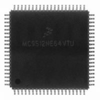
MC9S12NE64VTU Freescale Semiconductor, MC9S12NE64VTU Datasheet - Page 64

MC9S12NE64VTU
Manufacturer Part Number
MC9S12NE64VTU
Description
IC MCU 25MHZ ETHERNET/PHY 80TQFP
Manufacturer
Freescale Semiconductor
Series
HCS12r
Datasheet
1.MC9S12NE64VTU.pdf
(554 pages)
Specifications of MC9S12NE64VTU
Mfg Application Notes
MC9S12NE64 Integrated Ethernet Controller Implementing an Ethernet Interface with the MC9S12NE64 Web Server Development with MC9S12NE64 and Open TCP
Core Processor
HCS12
Core Size
16-Bit
Speed
25MHz
Connectivity
EBI/EMI, Ethernet, I²C, SCI, SPI
Peripherals
POR, PWM, WDT
Number Of I /o
38
Program Memory Size
64KB (64K x 8)
Program Memory Type
FLASH
Ram Size
8K x 8
Voltage - Supply (vcc/vdd)
2.375 V ~ 3.465 V
Data Converters
A/D 8x10b
Oscillator Type
Internal
Operating Temperature
-40°C ~ 105°C
Package / Case
80-TQFP Exposed Pad, 80-eTQFP, 80-HTQFP, 80-VQFP
Data Bus Width
16 bit
Data Ram Size
8 KB
Interface Type
I2C, SCI, SPI
Maximum Clock Frequency
25 MHz
Number Of Programmable I/os
70
Number Of Timers
16 bit
Operating Supply Voltage
- 0.3 V to + 3 V
Maximum Operating Temperature
+ 105 C
Mounting Style
SMD/SMT
Minimum Operating Temperature
- 65 C
On-chip Adc
10 bit
For Use With
EVB9S12NE64E - BOARD EVAL FOR 9S12NE64DEMO9S12NE64E - DEMO BOARD FOR 9S12NE64
Lead Free Status / RoHS Status
Lead free / RoHS Compliant
Eeprom Size
-
Lead Free Status / Rohs Status
Details
Available stocks
Company
Part Number
Manufacturer
Quantity
Price
Company:
Part Number:
MC9S12NE64VTU
Manufacturer:
FREESCALE
Quantity:
1 831
Company:
Part Number:
MC9S12NE64VTU
Manufacturer:
Freescale Semiconductor
Quantity:
10 000
Company:
Part Number:
MC9S12NE64VTUE
Manufacturer:
Freescale Semiconductor
Quantity:
10 000
Part Number:
MC9S12NE64VTUE
Manufacturer:
FREESCALE
Quantity:
20 000
- Current page: 64 of 554
- Download datasheet (4Mb)
Chapter 1 MC9S12NE64 Device Overview
1.6.2
Resets are a subset of the interrupts featured
system reset are summarized in
1.6.2.1
1.6.2.2
When a reset occurs, MCU registers and control bits are changed to known start-up states. See the
respective module block description chapter for register reset states. See the MEBI block description
chapter for mode-dependent pin configuration of port A, B, E, and K out of reset.
See the PIM block description chapter for reset configurations of all peripheral module ports.
See
The RAM array is not automatically initialized out of reset.
1.7
This section contains information regarding how the modules are implemented on the MC9S12NE64
device.
1.7.1
On the MC9S12NE64, the V
regulator. If this pin is tied low, then V
PHY_VDDA must be supplied externally.
1.7.2
In both the 112-pin LQFP and the 80-pin TQFP-EP package versions, both internal V
2.5 V domain are bonded out on two sides of the device as two pin pairs (V
V
allows systems to employ better supply routing and further decoupling.
64
DD1
Table 1-1
and V
Block Configuration for MC9S12NE64
Resets
V
V
DD2
Reset Summary Table
Effects of Reset
DDR
DD1
COP watchdog reset
Clock monitor reset
for locations of the memories depending on the operating mode after reset.
Low-voltage reset
Power-on reset
External reset
are connected together internally. V
, V
/V
Reset
REGEN
DD2
, V
DDR
SS1
Table
/V
, V
REGEN
SS2
MC9S12NE64 Data Sheet, Rev 1.0
1-8.
Priority
DD1
Table 1-8. Reset Summary
1
1
1
2
3
pin is used to enable or disable the internal voltage 3.3V to 2.5V
, V
inTable
DD2
, V
SS1
DDPLL
1-7. The different sources capable of generating a
VREG_PHY module
and V
CRG module
CRG module
CRG module
RESET pin
Source
, PHY_VDDRX, PHY_VDDTX, and
SS2
are connected together internally. This
DD1
$FFFE, $FFFF
$FFFE, $FFFF
$FFFE, $FFFF
$FFFC, $FFFD
$FFFA, $FFFB
/V
SS1
Freescale Semiconductor
Vector
DD
and V
and V
DD2
SS
/V
of the
SS2
).
Related parts for MC9S12NE64VTU
Image
Part Number
Description
Manufacturer
Datasheet
Request
R
Part Number:
Description:
Manufacturer:
Freescale Semiconductor, Inc
Datasheet:
Part Number:
Description:
Manufacturer:
Freescale Semiconductor, Inc
Datasheet:
Part Number:
Description:
Manufacturer:
Freescale Semiconductor, Inc
Datasheet:
Part Number:
Description:
Manufacturer:
Freescale Semiconductor, Inc
Datasheet:
Part Number:
Description:
Manufacturer:
Freescale Semiconductor, Inc
Datasheet:
Part Number:
Description:
Manufacturer:
Freescale Semiconductor, Inc
Datasheet:
Part Number:
Description:
Manufacturer:
Freescale Semiconductor, Inc
Datasheet:
Part Number:
Description:
Manufacturer:
Freescale Semiconductor, Inc
Datasheet:
Part Number:
Description:
Manufacturer:
Freescale Semiconductor, Inc
Datasheet:
Part Number:
Description:
Manufacturer:
Freescale Semiconductor, Inc
Datasheet:
Part Number:
Description:
Manufacturer:
Freescale Semiconductor, Inc
Datasheet:
Part Number:
Description:
Manufacturer:
Freescale Semiconductor, Inc
Datasheet:
Part Number:
Description:
Manufacturer:
Freescale Semiconductor, Inc
Datasheet:
Part Number:
Description:
Manufacturer:
Freescale Semiconductor, Inc
Datasheet:
Part Number:
Description:
Manufacturer:
Freescale Semiconductor, Inc
Datasheet:


