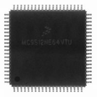
MC9S12NE64VTU Freescale Semiconductor, MC9S12NE64VTU Datasheet - Page 399

MC9S12NE64VTU
Manufacturer Part Number
MC9S12NE64VTU
Description
IC MCU 25MHZ ETHERNET/PHY 80TQFP
Manufacturer
Freescale Semiconductor
Series
HCS12r
Datasheet
1.MC9S12NE64VTU.pdf
(554 pages)
Specifications of MC9S12NE64VTU
Mfg Application Notes
MC9S12NE64 Integrated Ethernet Controller Implementing an Ethernet Interface with the MC9S12NE64 Web Server Development with MC9S12NE64 and Open TCP
Core Processor
HCS12
Core Size
16-Bit
Speed
25MHz
Connectivity
EBI/EMI, Ethernet, I²C, SCI, SPI
Peripherals
POR, PWM, WDT
Number Of I /o
38
Program Memory Size
64KB (64K x 8)
Program Memory Type
FLASH
Ram Size
8K x 8
Voltage - Supply (vcc/vdd)
2.375 V ~ 3.465 V
Data Converters
A/D 8x10b
Oscillator Type
Internal
Operating Temperature
-40°C ~ 105°C
Package / Case
80-TQFP Exposed Pad, 80-eTQFP, 80-HTQFP, 80-VQFP
Data Bus Width
16 bit
Data Ram Size
8 KB
Interface Type
I2C, SCI, SPI
Maximum Clock Frequency
25 MHz
Number Of Programmable I/os
70
Number Of Timers
16 bit
Operating Supply Voltage
- 0.3 V to + 3 V
Maximum Operating Temperature
+ 105 C
Mounting Style
SMD/SMT
Minimum Operating Temperature
- 65 C
On-chip Adc
10 bit
For Use With
EVB9S12NE64E - BOARD EVAL FOR 9S12NE64DEMO9S12NE64E - DEMO BOARD FOR 9S12NE64
Lead Free Status / RoHS Status
Lead free / RoHS Compliant
Eeprom Size
-
Lead Free Status / Rohs Status
Details
Available stocks
Company
Part Number
Manufacturer
Quantity
Price
Company:
Part Number:
MC9S12NE64VTU
Manufacturer:
FREESCALE
Quantity:
1 831
Company:
Part Number:
MC9S12NE64VTU
Manufacturer:
Freescale Semiconductor
Quantity:
10 000
Company:
Part Number:
MC9S12NE64VTUE
Manufacturer:
Freescale Semiconductor
Quantity:
10 000
Part Number:
MC9S12NE64VTUE
Manufacturer:
FREESCALE
Quantity:
20 000
- Current page: 399 of 554
- Download datasheet (4Mb)
Detailed descriptions of these pins can be found in the device overview chapter.
15.3
A summary of the registers associated with the MEBI sub-block is shown in
descriptions of the registers and bits are given in the subsections that follow. On most chips the registers
are mappable. Therefore, the upper bits may not be all 0s as shown in the table and descriptions.
Freescale Semiconductor
PE4/ECLK
PE3/LSTRB/ TAGLO
PE2/R/W
PE1/IRQ
PE0/XIRQ
PK7/ECS
PK6/XCS
PK5/X19
thru
PK0/X14
Pin Name
Memory Map and Register Definition
Table 15-1. External System Pins Associated With MEBI (continued)
PE4
ECLK
PE3
LSTRB
SZ8
TAGLO
PE2
R/W
PE1
IRQ
PE0
XIRQ
PK7
ECS
PK6
XCS
PK5–PK0
X19–X14
Pin Functions
MC9S12NE64 Data Sheet, Rev. 1.1
General-purpose I/O pin, see PORTE and DDRE registers.
Bus timing reference clock, can operate as a free-running clock at the system
clock rate or to produce one low-high clock per visible access, with the high
period stretched for slow accesses. ECLK is controlled by the NECLK bit in
PEAR, the IVIS bit in MODE, and the ESTR bit in EBICTL.
General-purpose I/O pin, see PORTE and DDRE registers.
Low strobe bar, 0 indicates valid data on D7–D0.
In special peripheral mode, this pin is an input indicating the size of the data
transfer (0 = 16-bit; 1 = 8-bit).
In expanded wide mode or emulation narrow modes, when instruction tagging
is on and low strobe is enabled, a 0 at the falling edge of E tags the low half of
the instruction word being read into the instruction queue.
General-purpose I/O pin, see PORTE and DDRE registers.
Read/write, indicates the direction of internal data transfers. This is an output
except in special peripheral mode where it is an input.
General-purpose input-only pin, can be read even if IRQ enabled.
Maskable interrupt request, can be level sensitive or edge sensitive.
General-purpose input-only pin.
Non-maskable interrupt input.
General-purpose I/O pin, see PORTK and DDRK registers.
Emulation chip select
General-purpose I/O pin, see PORTK and DDRK registers.
External data chip select
General-purpose I/O pins, see PORTK and DDRK registers.
Memory expansion addresses
Description
Memory Map and Register Definition
Table
15-2. Detailed
399
Related parts for MC9S12NE64VTU
Image
Part Number
Description
Manufacturer
Datasheet
Request
R
Part Number:
Description:
Manufacturer:
Freescale Semiconductor, Inc
Datasheet:
Part Number:
Description:
Manufacturer:
Freescale Semiconductor, Inc
Datasheet:
Part Number:
Description:
Manufacturer:
Freescale Semiconductor, Inc
Datasheet:
Part Number:
Description:
Manufacturer:
Freescale Semiconductor, Inc
Datasheet:
Part Number:
Description:
Manufacturer:
Freescale Semiconductor, Inc
Datasheet:
Part Number:
Description:
Manufacturer:
Freescale Semiconductor, Inc
Datasheet:
Part Number:
Description:
Manufacturer:
Freescale Semiconductor, Inc
Datasheet:
Part Number:
Description:
Manufacturer:
Freescale Semiconductor, Inc
Datasheet:
Part Number:
Description:
Manufacturer:
Freescale Semiconductor, Inc
Datasheet:
Part Number:
Description:
Manufacturer:
Freescale Semiconductor, Inc
Datasheet:
Part Number:
Description:
Manufacturer:
Freescale Semiconductor, Inc
Datasheet:
Part Number:
Description:
Manufacturer:
Freescale Semiconductor, Inc
Datasheet:
Part Number:
Description:
Manufacturer:
Freescale Semiconductor, Inc
Datasheet:
Part Number:
Description:
Manufacturer:
Freescale Semiconductor, Inc
Datasheet:
Part Number:
Description:
Manufacturer:
Freescale Semiconductor, Inc
Datasheet:


