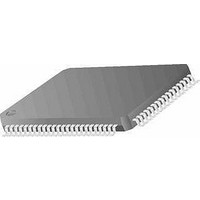
MC9S12E128CFU Freescale Semiconductor, MC9S12E128CFU Datasheet - Page 290

MC9S12E128CFU
Manufacturer Part Number
MC9S12E128CFU
Description
IC MCU 128K FLASH 25MHZ 80-QFP
Manufacturer
Freescale Semiconductor
Series
HCS12r
Specifications of MC9S12E128CFU
Core Processor
HCS12
Core Size
16-Bit
Speed
25MHz
Connectivity
EBI/EMI, I²C, SCI, SPI
Peripherals
POR, PWM, WDT
Number Of I /o
60
Program Memory Size
128KB (128K x 8)
Program Memory Type
FLASH
Ram Size
8K x 8
Voltage - Supply (vcc/vdd)
2.35 V ~ 2.75 V
Data Converters
A/D 16x10b; D/A 2x8b
Oscillator Type
Internal
Operating Temperature
-40°C ~ 85°C
Package / Case
80-QFP
Data Bus Width
16 bit
Data Ram Size
8 KB
Interface Type
SCI, SPI
Maximum Clock Frequency
25 MHz
Number Of Programmable I/os
60
Number Of Timers
16 bit
Operating Supply Voltage
3.135 V to 5.5 V
Maximum Operating Temperature
+ 85 C
Mounting Style
SMD/SMT
Minimum Operating Temperature
- 40 C
On-chip Adc
10 bit
On-chip Dac
8 bit, 2 Channel
For Use With
M68EVB912E128 - BOARD EVAL FOR MC9S12E128/64
Lead Free Status / RoHS Status
Contains lead / RoHS non-compliant
Eeprom Size
-
Lead Free Status / Rohs Status
No RoHS Version Available
Available stocks
Company
Part Number
Manufacturer
Quantity
Price
Company:
Part Number:
MC9S12E128CFU
Manufacturer:
FREESCALE
Quantity:
3
Company:
Part Number:
MC9S12E128CFU
Manufacturer:
Freescale Semiconductor
Quantity:
10 000
Part Number:
MC9S12E128CFU
Manufacturer:
FRE/MOT
Quantity:
20 000
Company:
Part Number:
MC9S12E128CFUE
Manufacturer:
FREESCALE
Quantity:
1 000
Company:
Part Number:
MC9S12E128CFUE
Manufacturer:
FREESCALE
Quantity:
5 530
Company:
Part Number:
MC9S12E128CFUE
Manufacturer:
Freescale Semiconductor
Quantity:
10 000
- Current page: 290 of 606
- Download datasheet (4Mb)
Chapter 9 Serial Peripheral Interface (SPIV3)
9.4.3
During an SPI transmission, data is transmitted (shifted out serially) and received (shifted in serially)
simultaneously. The serial clock (SCK) synchronizes shifting and sampling of the information on the two
serial data lines. A slave select line allows selection of an individual slave SPI device, slave devices that
are not selected do not interfere with SPI bus activities. Optionally, on a master SPI device, the slave select
line can be used to indicate multiple-master bus contention.
9.4.3.1
Using two bits in the SPI Control Register1, software selects one of four combinations of serial clock phase
and polarity.
The CPOL clock polarity control bit specifies an active high or low clock and has no significant effect on
the transmission format.
The CPHA clock phase control bit selects one of two fundamentally different transmission formats.
Clock phase and polarity should be identical for the master SPI device and the communicating slave
device. In some cases, the phase and polarity are changed between transmissions to allow a master device
to communicate with peripheral slaves having different requirements.
9.4.3.2
The first edge on the SCK line is used to clock the first data bit of the slave into the master and the first
data bit of the master into the slave. In some peripherals, the first bit of the slave’s data is available at the
slave’s data out pin as soon as the slave is selected. In this format, the first SCK edge is issued a half cycle
after SS has become low.
A half SCK cycle later, the second edge appears on the SCK line. When this second edge occurs, the value
previously latched from the serial data input pin is shifted into the LSB or MSB of the shift register,
depending on LSBFE bit.
After this second edge, the next bit of the SPI master data is transmitted out of the serial data output pin of
the master to the serial input pin on the slave. This process continues for a total of 16 edges on the SCK
line, with data being latched on odd numbered edges and shifted on even numbered edges.
290
Transmission Formats
Clock Phase and Polarity Controls
CPHA = 0 Transfer Format
SHIFT REGISTER
GENERATOR
BAUD RATE
MASTER SPI
Figure 9-8. Master/Slave Transfer Block Diagram
MC9S12E128 Data Sheet, Rev. 1.07
MISO
MOSI
SCK
SS
V
DD
MISO
MOSI
SCK
SS
SHIFT REGISTER
SLAVE SPI
Freescale Semiconductor
Related parts for MC9S12E128CFU
Image
Part Number
Description
Manufacturer
Datasheet
Request
R
Part Number:
Description:
Manufacturer:
Freescale Semiconductor, Inc
Datasheet:
Part Number:
Description:
Manufacturer:
Freescale Semiconductor, Inc
Datasheet:
Part Number:
Description:
Manufacturer:
Freescale Semiconductor, Inc
Datasheet:
Part Number:
Description:
Manufacturer:
Freescale Semiconductor, Inc
Datasheet:
Part Number:
Description:
Manufacturer:
Freescale Semiconductor, Inc
Datasheet:
Part Number:
Description:
Manufacturer:
Freescale Semiconductor, Inc
Datasheet:
Part Number:
Description:
Manufacturer:
Freescale Semiconductor, Inc
Datasheet:
Part Number:
Description:
Manufacturer:
Freescale Semiconductor, Inc
Datasheet:
Part Number:
Description:
Manufacturer:
Freescale Semiconductor, Inc
Datasheet:
Part Number:
Description:
Manufacturer:
Freescale Semiconductor, Inc
Datasheet:
Part Number:
Description:
Manufacturer:
Freescale Semiconductor, Inc
Datasheet:
Part Number:
Description:
Manufacturer:
Freescale Semiconductor, Inc
Datasheet:
Part Number:
Description:
Manufacturer:
Freescale Semiconductor, Inc
Datasheet:
Part Number:
Description:
Manufacturer:
Freescale Semiconductor, Inc
Datasheet:
Part Number:
Description:
Manufacturer:
Freescale Semiconductor, Inc
Datasheet:


