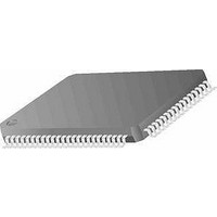
MC9S12E128CFU Freescale Semiconductor, MC9S12E128CFU Datasheet - Page 367

MC9S12E128CFU
Manufacturer Part Number
MC9S12E128CFU
Description
IC MCU 128K FLASH 25MHZ 80-QFP
Manufacturer
Freescale Semiconductor
Series
HCS12r
Specifications of MC9S12E128CFU
Core Processor
HCS12
Core Size
16-Bit
Speed
25MHz
Connectivity
EBI/EMI, I²C, SCI, SPI
Peripherals
POR, PWM, WDT
Number Of I /o
60
Program Memory Size
128KB (128K x 8)
Program Memory Type
FLASH
Ram Size
8K x 8
Voltage - Supply (vcc/vdd)
2.35 V ~ 2.75 V
Data Converters
A/D 16x10b; D/A 2x8b
Oscillator Type
Internal
Operating Temperature
-40°C ~ 85°C
Package / Case
80-QFP
Data Bus Width
16 bit
Data Ram Size
8 KB
Interface Type
SCI, SPI
Maximum Clock Frequency
25 MHz
Number Of Programmable I/os
60
Number Of Timers
16 bit
Operating Supply Voltage
3.135 V to 5.5 V
Maximum Operating Temperature
+ 85 C
Mounting Style
SMD/SMT
Minimum Operating Temperature
- 40 C
On-chip Adc
10 bit
On-chip Dac
8 bit, 2 Channel
For Use With
M68EVB912E128 - BOARD EVAL FOR MC9S12E128/64
Lead Free Status / RoHS Status
Contains lead / RoHS non-compliant
Eeprom Size
-
Lead Free Status / Rohs Status
No RoHS Version Available
Available stocks
Company
Part Number
Manufacturer
Quantity
Price
Company:
Part Number:
MC9S12E128CFU
Manufacturer:
FREESCALE
Quantity:
3
Company:
Part Number:
MC9S12E128CFU
Manufacturer:
Freescale Semiconductor
Quantity:
10 000
Part Number:
MC9S12E128CFU
Manufacturer:
FRE/MOT
Quantity:
20 000
Company:
Part Number:
MC9S12E128CFUE
Manufacturer:
FREESCALE
Quantity:
1 000
Company:
Part Number:
MC9S12E128CFUE
Manufacturer:
FREESCALE
Quantity:
5 530
Company:
Part Number:
MC9S12E128CFUE
Manufacturer:
Freescale Semiconductor
Quantity:
10 000
- Current page: 367 of 606
- Download datasheet (4Mb)
If both D flip-flops latch low, DT0 = 0, DT1 = 0, during deadtime periods if current is large and flowing
out of the complementary circuit. See
during deadtime periods if current is also large and flowing into the complementary circuit. However,
under low-current, the output voltage of the complementary circuit during deadtime is somewhere between
the high and low levels. The current cannot free-wheel throughout the opposition anti-body diode,
regardless of polarity, giving additional distortion when the current crosses zero. Sampled results will be
DT0 = 0 and DT1 = 1. Thus, the best time to change one PWM value register to another is just before the
current zero crossing.
Freescale Semiconductor
HIGH NEGATIVE CURRENT
HIGH POSITIVE CURRENT
LOW POSITIVE CURRENT
PWM0
PWM1
LOAD VOLTAGE WITH
LOAD VOLTAGE WITH
LOAD VOLTAGE WITH
LOAD VOLTAGE WITH
NEGATIVE CURRENT
PWM TO BOTTOM
Figure 11-55. Current-Status Sense Scheme for Deadtime Correction
TRANSISTOR
TRANSISTOR
PWM TO TOP
DEADTIME
T = DEADTIME INTERVAL BEFORE ASSERTION OF TOP PWM
B = DEADTIME INTERVAL BEFORE ASSERTION OF BOTTOM PWM
Figure 11-56. Output Voltage Waveforms
NEGATIVE
CURRENT
POSITIVE
CURRENT
MC9S12E128 Data Sheet, Rev. 1.07
Figure
T
VOLTAGE
SENSOR
11-55. If both D flip-flops latch the high, DT0 = 1, DT1 = 1,
B
Chapter 11 Pulse Width Modulator with Fault Protection (PMF15B6CV2)
IS0 PIN
T
PWM0
PWM1
B
D
D
CLK
CLK
Q
Q
V+
DT0
DT1
POSITIVE
CURRENT
NEGATIVE
CURRENT
367
Related parts for MC9S12E128CFU
Image
Part Number
Description
Manufacturer
Datasheet
Request
R
Part Number:
Description:
Manufacturer:
Freescale Semiconductor, Inc
Datasheet:
Part Number:
Description:
Manufacturer:
Freescale Semiconductor, Inc
Datasheet:
Part Number:
Description:
Manufacturer:
Freescale Semiconductor, Inc
Datasheet:
Part Number:
Description:
Manufacturer:
Freescale Semiconductor, Inc
Datasheet:
Part Number:
Description:
Manufacturer:
Freescale Semiconductor, Inc
Datasheet:
Part Number:
Description:
Manufacturer:
Freescale Semiconductor, Inc
Datasheet:
Part Number:
Description:
Manufacturer:
Freescale Semiconductor, Inc
Datasheet:
Part Number:
Description:
Manufacturer:
Freescale Semiconductor, Inc
Datasheet:
Part Number:
Description:
Manufacturer:
Freescale Semiconductor, Inc
Datasheet:
Part Number:
Description:
Manufacturer:
Freescale Semiconductor, Inc
Datasheet:
Part Number:
Description:
Manufacturer:
Freescale Semiconductor, Inc
Datasheet:
Part Number:
Description:
Manufacturer:
Freescale Semiconductor, Inc
Datasheet:
Part Number:
Description:
Manufacturer:
Freescale Semiconductor, Inc
Datasheet:
Part Number:
Description:
Manufacturer:
Freescale Semiconductor, Inc
Datasheet:
Part Number:
Description:
Manufacturer:
Freescale Semiconductor, Inc
Datasheet:


