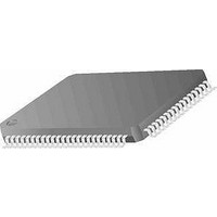
MC9S12E128CFU Freescale Semiconductor, MC9S12E128CFU Datasheet - Page 68

MC9S12E128CFU
Manufacturer Part Number
MC9S12E128CFU
Description
IC MCU 128K FLASH 25MHZ 80-QFP
Manufacturer
Freescale Semiconductor
Series
HCS12r
Specifications of MC9S12E128CFU
Core Processor
HCS12
Core Size
16-Bit
Speed
25MHz
Connectivity
EBI/EMI, I²C, SCI, SPI
Peripherals
POR, PWM, WDT
Number Of I /o
60
Program Memory Size
128KB (128K x 8)
Program Memory Type
FLASH
Ram Size
8K x 8
Voltage - Supply (vcc/vdd)
2.35 V ~ 2.75 V
Data Converters
A/D 16x10b; D/A 2x8b
Oscillator Type
Internal
Operating Temperature
-40°C ~ 85°C
Package / Case
80-QFP
Data Bus Width
16 bit
Data Ram Size
8 KB
Interface Type
SCI, SPI
Maximum Clock Frequency
25 MHz
Number Of Programmable I/os
60
Number Of Timers
16 bit
Operating Supply Voltage
3.135 V to 5.5 V
Maximum Operating Temperature
+ 85 C
Mounting Style
SMD/SMT
Minimum Operating Temperature
- 40 C
On-chip Adc
10 bit
On-chip Dac
8 bit, 2 Channel
For Use With
M68EVB912E128 - BOARD EVAL FOR MC9S12E128/64
Lead Free Status / RoHS Status
Contains lead / RoHS non-compliant
Eeprom Size
-
Lead Free Status / Rohs Status
No RoHS Version Available
Available stocks
Company
Part Number
Manufacturer
Quantity
Price
Company:
Part Number:
MC9S12E128CFU
Manufacturer:
FREESCALE
Quantity:
3
Company:
Part Number:
MC9S12E128CFU
Manufacturer:
Freescale Semiconductor
Quantity:
10 000
Part Number:
MC9S12E128CFU
Manufacturer:
FRE/MOT
Quantity:
20 000
Company:
Part Number:
MC9S12E128CFUE
Manufacturer:
FREESCALE
Quantity:
1 000
Company:
Part Number:
MC9S12E128CFUE
Manufacturer:
FREESCALE
Quantity:
5 530
Company:
Part Number:
MC9S12E128CFUE
Manufacturer:
Freescale Semiconductor
Quantity:
10 000
- Current page: 68 of 606
- Download datasheet (4Mb)
Chapter 1 MC9S12E128 Device Overview (MC9S12E128DGV1)
also be configured as Keypad Wake-up pins (KWU) and generate interrupts causing the MCU to exit STOP
or WAIT mode. Consult the Port Integration Module (PIM) PIM_9E128 block description chapter and the
ATD_10B16C block description chapter for information about pin configurations.
1.4.20
PM7 is a general purpose input or output pin. When the IIC module is enabled it becomes the serial clock
line (SCL) for the IIC module (IIC). While in reset and immediately out of reset the PM7 pin is configured
as a high impedance input pin. Consult the Port Integration Module (PIM) PIM_9E128 block description
chapter and the IIC block description chapter for information about pin configurations.
1.4.21
PM6 is a general purpose input or output pin. When the IIC module is enabled it becomes the Serial Data
Line (SDL) for the IIC module (IIC). While in reset and immediately out of reset the PM6 pin is configured
as a high impedance input pin. Consult the Port Integration Module (PIM) PIM_9E128 block description
chapter and the IIC block description chapter for information about pin configurations.
1.4.22
PM5 is a general purpose input or output. When the Serial Communications Interface 2 (SCI2) transmitter
is enabled the PM5 pin is configured as the transmit pin TXD2 of SCI2. While in reset and immediately
out of reset the PM5 pin is configured as a high impedance input pin. Consult the Port Integration Module
(PIM) PIM_9E128 block description chapter and the SCI block description chapter for information about
pin configurations.
1.4.23
PM4 is a general purpose input or output. When the Serial Communications Interface 2 (SCI2) receiver is
enabled the PM4 pin is configured as the receive pin RXD2 of SCI2. While in reset and immediately out
of reset the PM4 pin is configured as a high impedance input pin. Consult the Port Integration Module
(PIM) PIM_9E128 block description chapter and the SCI block description chapter for information about
pin configurations.
1.4.24
PM3 is a general purpose input or output pin. While in reset and immediately out of reset the PM3 pin is
configured as a high impedance input pin. Consult the Port Integration Module (PIM) PIM_9E128 block
description chapter for information about pin configurations.
1.4.25
PM1 is a general purpose input or output pin. When the Digital to Analog module 1 (DAC1) is enabled the
PM1 pin is configured as the analog output DA01 of DAC1. While in reset and immediately out of reset
the PM1 pin is configured as a high impedance input pin. Consult the Port Integration Module (PIM)
68
PM7 / SCL — Port M I/O Pin 7
PM6 / SDA — Port M I/O Pin 6
PM5 / TXD2 — Port M I/O Pin 5
PM4 / RXD2 — Port M I/O Pin 4
PM3 — Port M I/O Pin 3
PM1 / DAO1 — Port M I/O Pin 1
MC9S12E128 Data Sheet, Rev. 1.07
Freescale Semiconductor
Related parts for MC9S12E128CFU
Image
Part Number
Description
Manufacturer
Datasheet
Request
R
Part Number:
Description:
Manufacturer:
Freescale Semiconductor, Inc
Datasheet:
Part Number:
Description:
Manufacturer:
Freescale Semiconductor, Inc
Datasheet:
Part Number:
Description:
Manufacturer:
Freescale Semiconductor, Inc
Datasheet:
Part Number:
Description:
Manufacturer:
Freescale Semiconductor, Inc
Datasheet:
Part Number:
Description:
Manufacturer:
Freescale Semiconductor, Inc
Datasheet:
Part Number:
Description:
Manufacturer:
Freescale Semiconductor, Inc
Datasheet:
Part Number:
Description:
Manufacturer:
Freescale Semiconductor, Inc
Datasheet:
Part Number:
Description:
Manufacturer:
Freescale Semiconductor, Inc
Datasheet:
Part Number:
Description:
Manufacturer:
Freescale Semiconductor, Inc
Datasheet:
Part Number:
Description:
Manufacturer:
Freescale Semiconductor, Inc
Datasheet:
Part Number:
Description:
Manufacturer:
Freescale Semiconductor, Inc
Datasheet:
Part Number:
Description:
Manufacturer:
Freescale Semiconductor, Inc
Datasheet:
Part Number:
Description:
Manufacturer:
Freescale Semiconductor, Inc
Datasheet:
Part Number:
Description:
Manufacturer:
Freescale Semiconductor, Inc
Datasheet:
Part Number:
Description:
Manufacturer:
Freescale Semiconductor, Inc
Datasheet:


