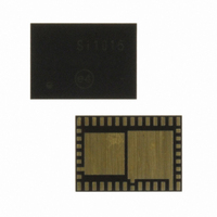
SI1000-C-GM Silicon Laboratories Inc, SI1000-C-GM Datasheet - Page 142

SI1000-C-GM
Manufacturer Part Number
SI1000-C-GM
Description
IC TXRX MCU + EZRADIOPRO
Manufacturer
Silicon Laboratories Inc
Specifications of SI1000-C-GM
Package / Case
42-QFN
Frequency
240MHz ~ 960MHz
Data Rate - Maximum
256kbps
Modulation Or Protocol
FSK, GFSK, OOK
Applications
General Purpose
Power - Output
20dBm
Sensitivity
-121dBm
Voltage - Supply
1.8 V ~ 3.6 V
Current - Receiving
18.5mA
Current - Transmitting
85mA
Data Interface
PCB, Surface Mount
Memory Size
64kB Flash, 4kB RAM
Antenna Connector
PCB, Surface Mount
Number Of Receivers
1
Number Of Transmitters
1
Wireless Frequency
240 MHz to 960 MHz
Interface Type
UART, SMBus, SPI, PCA
Output Power
20 dBm
Operating Supply Voltage
0.9 V to 3.6 V
Maximum Operating Temperature
+ 85 C
Mounting Style
SMD/SMT
Maximum Supply Current
4.1 mA
Minimum Operating Temperature
- 40 C
Modulation
FSK, GFSK, OOK
Protocol Supported
C2, SMBus
Core
8051
Program Memory Type
Flash
Program Memory Size
64 KB
Data Ram Size
4352 B
Supply Current (max)
4.1 mA
Cpu Family
Si100x
Device Core
8051
Device Core Size
8b
Frequency (max)
25MHz
Total Internal Ram Size
4.25KB
# I/os (max)
22
Number Of Timers - General Purpose
4
Operating Supply Voltage (typ)
2.5/3.3V
Operating Supply Voltage (max)
3.6V
Operating Supply Voltage (min)
1.8V
On-chip Adc
18-chx10-bit
Instruction Set Architecture
CISC
Mounting
Surface Mount
Pin Count
42
Package Type
QFN EP
Lead Free Status / RoHS Status
Lead free / RoHS Compliant
Operating Temperature
-
Lead Free Status / Rohs Status
Lead free / RoHS Compliant
Other names
336-1881-5
Available stocks
Company
Part Number
Manufacturer
Quantity
Price
Company:
Part Number:
SI1000-C-GM
Manufacturer:
FSC
Quantity:
1 000
- Current page: 142 of 376
- Download datasheet (3Mb)
Si1000/1/2/3/4/5
13.1.2. Flash Erase Procedure
The Flash memory is organized in 1024-byte pages. The erase operation applies to an entire page (setting
all bytes in the page to 0xFF). To erase an entire 1024-byte page, perform the following steps:
1. Save current interrupt state and disable interrupts.
2. Set the PSEE bit (register PSCTL).
3. Set the PSWE bit (register PSCTL).
4. Write the first key code to FLKEY: 0xA5.
5. Write the second key code to FLKEY: 0xF1.
6. Using the MOVX instruction, write a data byte to any location within the 1024-byte page to be erased.
7. Clear the PSWE and PSEE bits.
8. Restore previous interrupt state.
Steps 4–6 must be repeated for each 1024-byte page to be erased.
Notes:
13.1.3. Flash Write Procedure
A write to Flash memory can clear bits to logic 0 but cannot set them; only an erase operation can set bits
to logic 1 in Flash. A byte location to be programmed should be erased before a new value is written.
The recommended procedure for writing a single byte in Flash is as follows:
1. Save current interrupt state and disable interrupts.
2. Ensure that the Flash byte has been erased (has a value of 0xFF).
3. Set the PSWE bit (register PSCTL).
4. Clear the PSEE bit (register PSCTL).
5. Write the first key code to FLKEY: 0xA5.
6. Write the second key code to FLKEY: 0xF1.
7. Using the MOVX instruction, write a single data byte to the desired location within the 1024-byte sector.
8. Clear the PSWE bit.
9. Restore previous interrupt state.
Steps 5–7 must be repeated for each byte to be written.
Notes:
142
1. Future 16 and 8 kB derivatives in this product family will use a 512-byte page size. To maintain code
2. Flash security settings may prevent erasure of some Flash pages, such as the reserved area and the page
3. 8-bit MOVX instructions cannot be used to erase or write to Flash memory at addresses higher than 0x00FF.
1. Future 16 and 8 kB derivatives in this product family will use a 512-byte page size. To maintain code
2. Flash security settings may prevent writes to some areas of Flash, such as the reserved area. For a summary
compatibility across the entire family, the erase procedure should be performed on each 512-byte section of
memory.
containing the lock bytes. For a summary of Flash security settings and restrictions affecting Flash erase
operations, please see Section “13.3. Security Options” on page 143.
compatibility across the entire family, the erase procedure should be performed on each 512-byte section of
memory.
of Flash security settings and restrictions affecting Flash write operations, please see Section “13.3. Security
Options” on page 143.
Rev. 1.0
Related parts for SI1000-C-GM
Image
Part Number
Description
Manufacturer
Datasheet
Request
R
Part Number:
Description:
QFN 42/I�/915 MHZ, SNAP ENABLED PROGRAMABLE XCVR
Manufacturer:
Silicon Laboratories Inc
Part Number:
Description:
QFN 42/I�/64KB, 4KB RAM, +20 DBM, PROGRAMMABLE XCVR
Manufacturer:
Silicon Laboratories Inc
Part Number:
Description:
Microcontrollers (MCU) 915MHz SNAP enabled program XCVR
Manufacturer:
Silicon Laboratories Inc
Datasheet:

Part Number:
Description:
BOARD EVALUATION FOR SI1000
Manufacturer:
Silicon Laboratories Inc
Datasheet:

Part Number:
Description:
BOARD EVALUATION FOR SI1000
Manufacturer:
Silicon Laboratories Inc
Datasheet:

Part Number:
Description:
BOARD EVALUATION FOR SI1012
Manufacturer:
Silicon Laboratories Inc
Datasheet:

Part Number:
Description:
BOARD EVALUATION FOR SI1002
Manufacturer:
Silicon Laboratories Inc
Datasheet:

Part Number:
Description:
DEVELOPMENT KIT SI101X
Manufacturer:
Silicon Laboratories Inc
Datasheet:

Part Number:
Description:
BOARD EVALUATION FOR SI1004
Manufacturer:
Silicon Laboratories Inc
Datasheet:

Part Number:
Description:
BOARD EVALUATION FOR SI1004
Manufacturer:
Silicon Laboratories Inc
Datasheet:

Part Number:
Description:
BOARD EVALUATION FOR SI1012
Manufacturer:
Silicon Laboratories Inc
Datasheet:

Part Number:
Description:
BOARD EVALUATION FOR SI1014
Manufacturer:
Silicon Laboratories Inc
Datasheet:

Part Number:
Description:
DEVELOPMENT KIT SI101X
Manufacturer:
Silicon Laboratories Inc
Datasheet:


