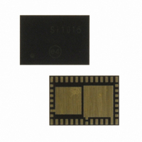
SI1000-C-GM Silicon Laboratories Inc, SI1000-C-GM Datasheet - Page 320

SI1000-C-GM
Manufacturer Part Number
SI1000-C-GM
Description
IC TXRX MCU + EZRADIOPRO
Manufacturer
Silicon Laboratories Inc
Specifications of SI1000-C-GM
Package / Case
42-QFN
Frequency
240MHz ~ 960MHz
Data Rate - Maximum
256kbps
Modulation Or Protocol
FSK, GFSK, OOK
Applications
General Purpose
Power - Output
20dBm
Sensitivity
-121dBm
Voltage - Supply
1.8 V ~ 3.6 V
Current - Receiving
18.5mA
Current - Transmitting
85mA
Data Interface
PCB, Surface Mount
Memory Size
64kB Flash, 4kB RAM
Antenna Connector
PCB, Surface Mount
Number Of Receivers
1
Number Of Transmitters
1
Wireless Frequency
240 MHz to 960 MHz
Interface Type
UART, SMBus, SPI, PCA
Output Power
20 dBm
Operating Supply Voltage
0.9 V to 3.6 V
Maximum Operating Temperature
+ 85 C
Mounting Style
SMD/SMT
Maximum Supply Current
4.1 mA
Minimum Operating Temperature
- 40 C
Modulation
FSK, GFSK, OOK
Protocol Supported
C2, SMBus
Core
8051
Program Memory Type
Flash
Program Memory Size
64 KB
Data Ram Size
4352 B
Supply Current (max)
4.1 mA
Cpu Family
Si100x
Device Core
8051
Device Core Size
8b
Frequency (max)
25MHz
Total Internal Ram Size
4.25KB
# I/os (max)
22
Number Of Timers - General Purpose
4
Operating Supply Voltage (typ)
2.5/3.3V
Operating Supply Voltage (max)
3.6V
Operating Supply Voltage (min)
1.8V
On-chip Adc
18-chx10-bit
Instruction Set Architecture
CISC
Mounting
Surface Mount
Pin Count
42
Package Type
QFN EP
Lead Free Status / RoHS Status
Lead free / RoHS Compliant
Operating Temperature
-
Lead Free Status / Rohs Status
Lead free / RoHS Compliant
Other names
336-1881-5
Available stocks
Company
Part Number
Manufacturer
Quantity
Price
Company:
Part Number:
SI1000-C-GM
Manufacturer:
FSC
Quantity:
1 000
- Current page: 320 of 376
- Download datasheet (3Mb)
Si1000/1/2/3/4/5
26.3. SPI0 Slave Mode Operation
When SPI0 is enabled and not configured as a master, it will operate as a SPI slave. As a slave, bytes are
shifted in through the MOSI pin and out through the MISO pin by a master device controlling the SCK
signal. A bit counter in the SPI0 logic counts SCK edges. When 8 bits have been shifted through the shift
register, the SPIF flag is set to logic 1, and the byte is copied into the receive buffer. Data is read from the
receive buffer by reading SPI0DAT. A slave device cannot initiate transfers. Data to be transferred to the
master device is pre-loaded into the shift register by writing to SPI0DAT. Writes to SPI0DAT are double-
buffered, and are placed in the transmit buffer first. If the shift register is empty, the contents of the transmit
buffer will immediately be transferred into the shift register. When the shift register already contains data,
the SPI will load the shift register with the transmit buffer’s contents after the last SCK edge of the next (or
current) SPI transfer.
When configured as a slave, SPI0 can be configured for 4-wire or 3-wire operation. The default, 4-wire
slave mode, is active when NSSMD1 (SPI0CN.3) = 0 and NSSMD0 (SPI0CN.2) = 1. In 4-wire mode, the
NSS signal is routed to a port pin and configured as a digital input. SPI0 is enabled when NSS is logic 0,
and disabled when NSS is logic 1. The bit counter is reset on a falling edge of NSS. Note that the NSS
signal must be driven low at least 2 system clocks before the first active edge of SCK for each byte
transfer. Figure 26.4 shows a connection diagram between two slave devices in 4-wire slave mode and a
master device.
3-wire slave mode is active when NSSMD1 (SPI0CN.3) = 0 and NSSMD0 (SPI0CN.2) = 0. NSS is not
used in this mode, and is not mapped to an external port pin through the crossbar. Since there is no way of
uniquely addressing the device in 3-wire slave mode, SPI0 must be the only slave device present on the
bus. It is important to note that in 3-wire slave mode there is no external means of resetting the bit counter
that determines when a full byte has been received. The bit counter can only be reset by disabling and re-
enabling SPI0 with the SPIEN bit. Figure 26.3 shows a connection diagram between a slave device in 3-
wire slave mode and a master device.
320
Figure 26.4. 4-Wire Single Master Mode and 4-Wire Slave Mode Connection Diagram
Master
Device
GPIO
MISO
MOSI
SCK
NSS
Rev. 1.0
MISO
MOSI
SCK
NSS
MISO
MOSI
SCK
NSS
Device
Device
Slave
Slave
Related parts for SI1000-C-GM
Image
Part Number
Description
Manufacturer
Datasheet
Request
R
Part Number:
Description:
QFN 42/I�/915 MHZ, SNAP ENABLED PROGRAMABLE XCVR
Manufacturer:
Silicon Laboratories Inc
Part Number:
Description:
QFN 42/I�/64KB, 4KB RAM, +20 DBM, PROGRAMMABLE XCVR
Manufacturer:
Silicon Laboratories Inc
Part Number:
Description:
Microcontrollers (MCU) 915MHz SNAP enabled program XCVR
Manufacturer:
Silicon Laboratories Inc
Datasheet:

Part Number:
Description:
BOARD EVALUATION FOR SI1000
Manufacturer:
Silicon Laboratories Inc
Datasheet:

Part Number:
Description:
BOARD EVALUATION FOR SI1000
Manufacturer:
Silicon Laboratories Inc
Datasheet:

Part Number:
Description:
BOARD EVALUATION FOR SI1012
Manufacturer:
Silicon Laboratories Inc
Datasheet:

Part Number:
Description:
BOARD EVALUATION FOR SI1002
Manufacturer:
Silicon Laboratories Inc
Datasheet:

Part Number:
Description:
DEVELOPMENT KIT SI101X
Manufacturer:
Silicon Laboratories Inc
Datasheet:

Part Number:
Description:
BOARD EVALUATION FOR SI1004
Manufacturer:
Silicon Laboratories Inc
Datasheet:

Part Number:
Description:
BOARD EVALUATION FOR SI1004
Manufacturer:
Silicon Laboratories Inc
Datasheet:

Part Number:
Description:
BOARD EVALUATION FOR SI1012
Manufacturer:
Silicon Laboratories Inc
Datasheet:

Part Number:
Description:
BOARD EVALUATION FOR SI1014
Manufacturer:
Silicon Laboratories Inc
Datasheet:

Part Number:
Description:
DEVELOPMENT KIT SI101X
Manufacturer:
Silicon Laboratories Inc
Datasheet:


