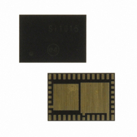
SI1000-C-GM Silicon Laboratories Inc, SI1000-C-GM Datasheet - Page 231

SI1000-C-GM
Manufacturer Part Number
SI1000-C-GM
Description
IC TXRX MCU + EZRADIOPRO
Manufacturer
Silicon Laboratories Inc
Specifications of SI1000-C-GM
Package / Case
42-QFN
Frequency
240MHz ~ 960MHz
Data Rate - Maximum
256kbps
Modulation Or Protocol
FSK, GFSK, OOK
Applications
General Purpose
Power - Output
20dBm
Sensitivity
-121dBm
Voltage - Supply
1.8 V ~ 3.6 V
Current - Receiving
18.5mA
Current - Transmitting
85mA
Data Interface
PCB, Surface Mount
Memory Size
64kB Flash, 4kB RAM
Antenna Connector
PCB, Surface Mount
Number Of Receivers
1
Number Of Transmitters
1
Wireless Frequency
240 MHz to 960 MHz
Interface Type
UART, SMBus, SPI, PCA
Output Power
20 dBm
Operating Supply Voltage
0.9 V to 3.6 V
Maximum Operating Temperature
+ 85 C
Mounting Style
SMD/SMT
Maximum Supply Current
4.1 mA
Minimum Operating Temperature
- 40 C
Modulation
FSK, GFSK, OOK
Protocol Supported
C2, SMBus
Core
8051
Program Memory Type
Flash
Program Memory Size
64 KB
Data Ram Size
4352 B
Supply Current (max)
4.1 mA
Cpu Family
Si100x
Device Core
8051
Device Core Size
8b
Frequency (max)
25MHz
Total Internal Ram Size
4.25KB
# I/os (max)
22
Number Of Timers - General Purpose
4
Operating Supply Voltage (typ)
2.5/3.3V
Operating Supply Voltage (max)
3.6V
Operating Supply Voltage (min)
1.8V
On-chip Adc
18-chx10-bit
Instruction Set Architecture
CISC
Mounting
Surface Mount
Pin Count
42
Package Type
QFN EP
Lead Free Status / RoHS Status
Lead free / RoHS Compliant
Operating Temperature
-
Lead Free Status / Rohs Status
Lead free / RoHS Compliant
Other names
336-1881-5
Available stocks
Company
Part Number
Manufacturer
Quantity
Price
Company:
Part Number:
SI1000-C-GM
Manufacturer:
FSC
Quantity:
1 000
- Current page: 231 of 376
- Download datasheet (3Mb)
SDO
SCLK
nSEL
SCLK
nSEL
SDI
SDI
MOSI
SCL
MISO
MOSI
SCL
NSS
NSS
The SPI interface contains a burst read/write mode which allows for reading/writing sequential registers
without having to re-send the SPI address. When the NSS bit is held low while continuing to send SCK
pulses, the SPI interface will automatically increment the ADDR and read from/write to the next address.
An example burst write transaction is illustrated in Figure 22.4 and a burst read in Figure 22.5. As long as
NSS is held low, input data will be latched into the transceiver every eight SCK cycles.
First Bit
First Bit
RW
RW
=1
=0
A6
A6
A5
A5
A4
A4
A3
A3
Figure 22.4. SPI Timing—Burst Write Mode
Figure 22.5. SPI Timing—Burst Read Mode
A2
A2
A1
A1
First Bit
A0
A0
D7
=X
D7
D7
=X
D6 D5 D4 D3
D6
=X
D6
=X
D5
=X
D5
=X
Rev. 1.0
D4
=X
D4
=X
D3
=X
D3
=X
D2
=X
D2
=X
D2 D1 D0
Last Bit
D1
=X
D1
=X
D0
=X
D0
=X
D7
=X
D7 D6 D5 D4 D3
Si1000/1/2/3/4/5
D6
=X
D5
=X
D4
=X
D3
=X
D2
=X
D2 D1 D0
D1
=X
Last Bit
D0
=X
231
Related parts for SI1000-C-GM
Image
Part Number
Description
Manufacturer
Datasheet
Request
R
Part Number:
Description:
QFN 42/I�/915 MHZ, SNAP ENABLED PROGRAMABLE XCVR
Manufacturer:
Silicon Laboratories Inc
Part Number:
Description:
QFN 42/I�/64KB, 4KB RAM, +20 DBM, PROGRAMMABLE XCVR
Manufacturer:
Silicon Laboratories Inc
Part Number:
Description:
Microcontrollers (MCU) 915MHz SNAP enabled program XCVR
Manufacturer:
Silicon Laboratories Inc
Datasheet:

Part Number:
Description:
BOARD EVALUATION FOR SI1000
Manufacturer:
Silicon Laboratories Inc
Datasheet:

Part Number:
Description:
BOARD EVALUATION FOR SI1000
Manufacturer:
Silicon Laboratories Inc
Datasheet:

Part Number:
Description:
BOARD EVALUATION FOR SI1012
Manufacturer:
Silicon Laboratories Inc
Datasheet:

Part Number:
Description:
BOARD EVALUATION FOR SI1002
Manufacturer:
Silicon Laboratories Inc
Datasheet:

Part Number:
Description:
DEVELOPMENT KIT SI101X
Manufacturer:
Silicon Laboratories Inc
Datasheet:

Part Number:
Description:
BOARD EVALUATION FOR SI1004
Manufacturer:
Silicon Laboratories Inc
Datasheet:

Part Number:
Description:
BOARD EVALUATION FOR SI1004
Manufacturer:
Silicon Laboratories Inc
Datasheet:

Part Number:
Description:
BOARD EVALUATION FOR SI1012
Manufacturer:
Silicon Laboratories Inc
Datasheet:

Part Number:
Description:
BOARD EVALUATION FOR SI1014
Manufacturer:
Silicon Laboratories Inc
Datasheet:

Part Number:
Description:
DEVELOPMENT KIT SI101X
Manufacturer:
Silicon Laboratories Inc
Datasheet:


