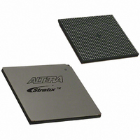
EP1S40B956C5 Altera, EP1S40B956C5 Datasheet - Page 340

EP1S40B956C5
Manufacturer Part Number
EP1S40B956C5
Description
IC STRATIX FPGA 40K LE 956-BGA
Manufacturer
Altera
Series
Stratix®r
Datasheet
1.EP1S10F484I6N.pdf
(864 pages)
Specifications of EP1S40B956C5
Number Of Logic Elements/cells
41250
Number Of Labs/clbs
4125
Total Ram Bits
3423744
Number Of I /o
683
Voltage - Supply
1.425 V ~ 1.575 V
Mounting Type
Surface Mount
Operating Temperature
0°C ~ 85°C
Package / Case
956-BGA
Lead Free Status / RoHS Status
Contains lead / RoHS non-compliant
Number Of Gates
-
Available stocks
Company
Part Number
Manufacturer
Quantity
Price
Part Number:
EP1S40B956C5
Manufacturer:
ALTERA/阿尔特拉
Quantity:
20 000
- Current page: 340 of 864
- Download datasheet (11Mb)
Enhanced PLLs
1–30
Stratix Device Handbook, Volume 2
CLK4p/n
CLK5p/n
CLK6p/n
CLK7p/n
CLK12p/n
CLK13p/n
CLK14p/n
CLK15p/n
PLL5_FBp/n
PLL6_FBp/n
PLLENABLE
Table 1–9. Enhanced PLL Pins (Part 1 of 2)
Pin
f
Single-ended or differential pins that can drive the inclk port for PLL 6.
Single-ended or differential pins that can drive the inclk port for PLL 6.
Single-ended or differential pins that can drive the inclk port for PLL 12.
Single-ended or differential pins that can drive the inclk port for PLL 12.
Single-ended or differential pins that can drive the inclk port for PLL 11.
Single-ended or differential pins that can drive the inclk port for PLL 11.
Single-ended or differential pins that can drive the inclk port for PLL 5.
Single-ended or differential pins that can drive the inclk port for PLL 5.
Single-ended or differential pins that can drive the fbin port for PLL 5.
Single-ended or differential pins that can drive the fbin port for PLL 6.
Dedicated input pin that drives the pllena port of all or a set of PLLs. If you do not
use this pin, connect it to ground.
With down-spread modulation, the peak of the modulated waveform is
the actual target frequency. Therefore, the system never exceeds the
maximum clock speed. To maintain reliable communication, the entire
system/subsystem should use the Stratix or Stratix GX device as the clock
source. Communication could fail if the Stratix or Stratix GX logic array
is clocked by the spread-spectrum clock, but the data it receives from
another device is not.
Since spread spectrum affects the m counter values, all spread-spectrum
PLL outputs are affected. Therefore, if only one spread-spectrum signal is
needed, the clock signal should use a separate PLL without other outputs
from that PLL.
No special considerations are needed when using spread spectrum with
the clock switchover feature. This is because the clock switchover feature
does not affect the m and n counter values, which are the counter values
that are switching when using spread spectrum.
PLL Reconfiguration
See AN 282: Implementing PLL Reconfiguration in Stratix & Stratix GX
Devices for information on PLL reconfiguration.
Enhanced PLL Pins
Table 1–9
PLLs. For inclk port connections to pins see
shows the physical pins and their purpose for the Enhanced
Description
“Clocking” on page
Altera Corporation
July 2005
1–39.
Related parts for EP1S40B956C5
Image
Part Number
Description
Manufacturer
Datasheet
Request
R

Part Number:
Description:
CYCLONE II STARTER KIT EP2C20N
Manufacturer:
Altera
Datasheet:

Part Number:
Description:
CPLD, EP610 Family, ECMOS Process, 300 Gates, 16 Macro Cells, 16 Reg., 16 User I/Os, 5V Supply, 35 Speed Grade, 24DIP
Manufacturer:
Altera Corporation
Datasheet:

Part Number:
Description:
CPLD, EP610 Family, ECMOS Process, 300 Gates, 16 Macro Cells, 16 Reg., 16 User I/Os, 5V Supply, 15 Speed Grade, 24DIP
Manufacturer:
Altera Corporation
Datasheet:

Part Number:
Description:
Manufacturer:
Altera Corporation
Datasheet:

Part Number:
Description:
CPLD, EP610 Family, ECMOS Process, 300 Gates, 16 Macro Cells, 16 Reg., 16 User I/Os, 5V Supply, 30 Speed Grade, 24DIP
Manufacturer:
Altera Corporation
Datasheet:

Part Number:
Description:
High-performance, low-power erasable programmable logic devices with 8 macrocells, 10ns
Manufacturer:
Altera Corporation
Datasheet:

Part Number:
Description:
High-performance, low-power erasable programmable logic devices with 8 macrocells, 7ns
Manufacturer:
Altera Corporation
Datasheet:

Part Number:
Description:
Classic EPLD
Manufacturer:
Altera Corporation
Datasheet:

Part Number:
Description:
High-performance, low-power erasable programmable logic devices with 8 macrocells, 10ns
Manufacturer:
Altera Corporation
Datasheet:

Part Number:
Description:
Manufacturer:
Altera Corporation
Datasheet:

Part Number:
Description:
Manufacturer:
Altera Corporation
Datasheet:

Part Number:
Description:
Manufacturer:
Altera Corporation
Datasheet:

Part Number:
Description:
CPLD, EP610 Family, ECMOS Process, 300 Gates, 16 Macro Cells, 16 Reg., 16 User I/Os, 5V Supply, 25 Speed Grade, 24DIP
Manufacturer:
Altera Corporation
Datasheet:


