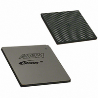
EP1S40B956C5 Altera, EP1S40B956C5 Datasheet - Page 468

EP1S40B956C5
Manufacturer Part Number
EP1S40B956C5
Description
IC STRATIX FPGA 40K LE 956-BGA
Manufacturer
Altera
Series
Stratix®r
Datasheet
1.EP1S10F484I6N.pdf
(864 pages)
Specifications of EP1S40B956C5
Number Of Logic Elements/cells
41250
Number Of Labs/clbs
4125
Total Ram Bits
3423744
Number Of I /o
683
Voltage - Supply
1.425 V ~ 1.575 V
Mounting Type
Surface Mount
Operating Temperature
0°C ~ 85°C
Package / Case
956-BGA
Lead Free Status / RoHS Status
Contains lead / RoHS non-compliant
Number Of Gates
-
Available stocks
Company
Part Number
Manufacturer
Quantity
Price
Part Number:
EP1S40B956C5
Manufacturer:
ALTERA/阿尔特拉
Quantity:
20 000
- Current page: 468 of 864
- Download datasheet (11Mb)
Quartus II Software Support
4–40
Stratix Device Handbook, Volume 2
When you assign an I/O standard that requires a reference voltage to an
I/O pin, the Quartus II software automatically assigns V
Quartus II Help for instructions on how to use an I/O standard for a pin.
Programmable Drive Strength Settings
To make programmable drive strength settings, perform the following
steps:
1.
2.
3.
4.
5.
6.
7.
I/O Banks in the Floorplan View
You can view the arrangement of the device I/O banks in the Floorplan
View (View menu) as shown in
standards to the I/O pins in any given I/O bank as long as the V
the standards is the same. Pins that belong to the same I/O bank must use
the same
Each device I/O pin belongs to a specific, numbered I/O bank. The
Quartus II software color codes the I/O bank to which each I/O pin and
V
bank color and the bank numbers for each pin.
CCIO
In the Tools menu, choose Assignment Organizer.
Choose the Edit specific entity & node settings for: setting, then
select the output or bidirectional pin to specify the current strength
for.
In the Assignment Categories dialog box, select Options for
Individual Nodes Only.
Select Click here to add a new assignment.
In the Assignment dialog box, set the Name field to Current
Strength and set the Setting field to the desired, allowable value.
Click Add.
Click Apply, then OK.
pin belong. Turn on the Show I/O Banks option to display the I/O
V
CCIO
signal.
Figure
4–24. You can assign multiple I/O
Altera Corporation
REF
pins. See the
June 2006
CCIO
of
Related parts for EP1S40B956C5
Image
Part Number
Description
Manufacturer
Datasheet
Request
R

Part Number:
Description:
CYCLONE II STARTER KIT EP2C20N
Manufacturer:
Altera
Datasheet:

Part Number:
Description:
CPLD, EP610 Family, ECMOS Process, 300 Gates, 16 Macro Cells, 16 Reg., 16 User I/Os, 5V Supply, 35 Speed Grade, 24DIP
Manufacturer:
Altera Corporation
Datasheet:

Part Number:
Description:
CPLD, EP610 Family, ECMOS Process, 300 Gates, 16 Macro Cells, 16 Reg., 16 User I/Os, 5V Supply, 15 Speed Grade, 24DIP
Manufacturer:
Altera Corporation
Datasheet:

Part Number:
Description:
Manufacturer:
Altera Corporation
Datasheet:

Part Number:
Description:
CPLD, EP610 Family, ECMOS Process, 300 Gates, 16 Macro Cells, 16 Reg., 16 User I/Os, 5V Supply, 30 Speed Grade, 24DIP
Manufacturer:
Altera Corporation
Datasheet:

Part Number:
Description:
High-performance, low-power erasable programmable logic devices with 8 macrocells, 10ns
Manufacturer:
Altera Corporation
Datasheet:

Part Number:
Description:
High-performance, low-power erasable programmable logic devices with 8 macrocells, 7ns
Manufacturer:
Altera Corporation
Datasheet:

Part Number:
Description:
Classic EPLD
Manufacturer:
Altera Corporation
Datasheet:

Part Number:
Description:
High-performance, low-power erasable programmable logic devices with 8 macrocells, 10ns
Manufacturer:
Altera Corporation
Datasheet:

Part Number:
Description:
Manufacturer:
Altera Corporation
Datasheet:

Part Number:
Description:
Manufacturer:
Altera Corporation
Datasheet:

Part Number:
Description:
Manufacturer:
Altera Corporation
Datasheet:

Part Number:
Description:
CPLD, EP610 Family, ECMOS Process, 300 Gates, 16 Macro Cells, 16 Reg., 16 User I/Os, 5V Supply, 25 Speed Grade, 24DIP
Manufacturer:
Altera Corporation
Datasheet:


