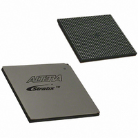
EP1S40B956C5 Altera, EP1S40B956C5 Datasheet - Page 532

EP1S40B956C5
Manufacturer Part Number
EP1S40B956C5
Description
IC STRATIX FPGA 40K LE 956-BGA
Manufacturer
Altera
Series
Stratix®r
Datasheet
1.EP1S10F484I6N.pdf
(864 pages)
Specifications of EP1S40B956C5
Number Of Logic Elements/cells
41250
Number Of Labs/clbs
4125
Total Ram Bits
3423744
Number Of I /o
683
Voltage - Supply
1.425 V ~ 1.575 V
Mounting Type
Surface Mount
Operating Temperature
0°C ~ 85°C
Package / Case
956-BGA
Lead Free Status / RoHS Status
Contains lead / RoHS non-compliant
Number Of Gates
-
Available stocks
Company
Part Number
Manufacturer
Quantity
Price
Part Number:
EP1S40B956C5
Manufacturer:
ALTERA/阿尔特拉
Quantity:
20 000
- Current page: 532 of 864
- Download datasheet (11Mb)
Software Support
5–60
Stratix Device Handbook, Volume 2
Notes to
(1)
(2)
(3)
(4)
rx_in[number_of_channels - 1..0]
rx_inclock
rx_pll_enable
rx_data_align
rx_locked
rx_out[Deserialization_factor *
number_of_channels -1..0]
rx_outclock
Table 5–15. LVDS Receiver Ports
This is an optional port.
Only one rx_pll_enable pin is necessary to enable all the PLLs in the device.
This is a non-differential pin.
See
alignment, you must synchronize rx_data_align with rx_outclock.
“Realignment Implementation” on page 5–28
Table
5–15:
Port Name
When you span two I/O banks using cross-bank support, you can route
only two load enable signals total between the plls. When you enable
rx_data_align, you use both rxloadena and txloadena of a PLL.
That leaves no loadena for the second PLL.
The only way you can use the rx_data_align is if one of the following
is true:
■
■
LVDS Receiver Block
You only need to enter the input clock frequency, deserialization factor,
and the input data rate to implement an LVDS receiver block. The
Quartus II software then automatically sets the clock boost (W) factor for
the receiver. In addition, you can also indicate the clock and data
alignment for the receiver or add the pll_enable, rx_data_align,
and rx_locked output ports.
available ports in the LVDS receiver block.
The RX PLL is only clocking RX channels (no resources for TX)
If all channels can fit in one I/O bank
Input
Input
Input
Input
Output
Output
Output
Direction
for more information. For guaranteed performance and data
Input data channel
Reference input clock
Enables fast PLL
Control for the data
realignment circuitry
Fast PLL locked pin
De-serialized data
Internal reference clock
Table 5–15
Function
explains the function of the
Pin
Pin or output from a PLL
Pin (1), (2),
Pin or logic array (1),
(3),
Pin or logic array (1),
Logic array
Logic array
Source/Output Port
(4)
Altera Corporation
Destination
Input Port
(3)
July 2005
(3)
Related parts for EP1S40B956C5
Image
Part Number
Description
Manufacturer
Datasheet
Request
R

Part Number:
Description:
CYCLONE II STARTER KIT EP2C20N
Manufacturer:
Altera
Datasheet:

Part Number:
Description:
CPLD, EP610 Family, ECMOS Process, 300 Gates, 16 Macro Cells, 16 Reg., 16 User I/Os, 5V Supply, 35 Speed Grade, 24DIP
Manufacturer:
Altera Corporation
Datasheet:

Part Number:
Description:
CPLD, EP610 Family, ECMOS Process, 300 Gates, 16 Macro Cells, 16 Reg., 16 User I/Os, 5V Supply, 15 Speed Grade, 24DIP
Manufacturer:
Altera Corporation
Datasheet:

Part Number:
Description:
Manufacturer:
Altera Corporation
Datasheet:

Part Number:
Description:
CPLD, EP610 Family, ECMOS Process, 300 Gates, 16 Macro Cells, 16 Reg., 16 User I/Os, 5V Supply, 30 Speed Grade, 24DIP
Manufacturer:
Altera Corporation
Datasheet:

Part Number:
Description:
High-performance, low-power erasable programmable logic devices with 8 macrocells, 10ns
Manufacturer:
Altera Corporation
Datasheet:

Part Number:
Description:
High-performance, low-power erasable programmable logic devices with 8 macrocells, 7ns
Manufacturer:
Altera Corporation
Datasheet:

Part Number:
Description:
Classic EPLD
Manufacturer:
Altera Corporation
Datasheet:

Part Number:
Description:
High-performance, low-power erasable programmable logic devices with 8 macrocells, 10ns
Manufacturer:
Altera Corporation
Datasheet:

Part Number:
Description:
Manufacturer:
Altera Corporation
Datasheet:

Part Number:
Description:
Manufacturer:
Altera Corporation
Datasheet:

Part Number:
Description:
Manufacturer:
Altera Corporation
Datasheet:

Part Number:
Description:
CPLD, EP610 Family, ECMOS Process, 300 Gates, 16 Macro Cells, 16 Reg., 16 User I/Os, 5V Supply, 25 Speed Grade, 24DIP
Manufacturer:
Altera Corporation
Datasheet:


