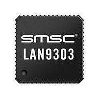
LAN9303-ABZJ SMSC, LAN9303-ABZJ Datasheet - Page 108

LAN9303-ABZJ
Manufacturer Part Number
LAN9303-ABZJ
Description
IC ETHER SW 3PORT 16BIT 56QFN
Manufacturer
SMSC
Specifications of LAN9303-ABZJ
Controller Type
Ethernet Switch Controller
Interface
SMBus (2-Wire/I²C)
Voltage - Supply
3 V ~ 3.6 V
Current - Supply
190mA
Operating Temperature
0°C ~ 70°C
Mounting Type
Surface Mount
Package / Case
56-QFN
Product
Ethernet Switches
Standard Supported
Yes
Data Rate
10 Mbps/100 Mbps
Supply Voltage (max)
3.6 V
Supply Voltage (min)
3 V
Supply Current (max)
0.19 A (Typ)
Maximum Operating Temperature
+ 70 C
Minimum Operating Temperature
0 C
Mounting Style
SMD/SMT
For Use With
638-1095 - EVALUATION BOARD FOR LAN9303
Lead Free Status / Rohs Status
Lead free / RoHS Compliant
Other names
638-1082
Available stocks
Company
Part Number
Manufacturer
Quantity
Price
Part Number:
LAN9303-ABZJ
Manufacturer:
MICROCHIP/微芯
Quantity:
20 000
- Current page: 108 of 367
- Download datasheet (4Mb)
Revision 1.4 (07-07-10)
8.3.1
8.3.2
S 1 0 1 0
A
C
K
S 1 0 1 0
Control Byte
Chip / Block
Select Bits
Control Byte
Chip / Block
Single Byte Addressing
A
1
0
Select Bits
I
The I
by the address byte or bytes. The control byte is preceded by a start condition. The control byte and
address byte(s) are each acknowledged by the EEPROM slave. If the EEPROM slave fails to send an
acknowledge, then the sequence is aborted and the
of the
The control byte consists of a 4-bit control code, 3-bits of chip/block select and one direction bit. The
control code is 1010b. For single byte addressing EEPROMs, the chip/block select bits are used for
address bits 10, 9, and 8. For double byte addressing EEPROMs, the chip/block select bits are set
low. The direction bit is set low to indicate the address is being written.
Figure 8.2
I
Following the device addressing, a data byte may be read from the EEPROM by outputting a start
condition and control byte with a control code of 1010b, chip/block select bits as described in
Section
bits of data. If the EEPROM slave fails to send an acknowledge, then the sequence is aborted and
the
(E2P_CMD)
Figure 8.3
For a register level description of a read operation, refer to
Controller Operation," on page
Single Byte Addressing Read
2
A
2
9
C EEPROM Device Addressing
C EEPROM Byte Read
A
8
A
1
0
EEPROM Controller Timeout (EPC_TIMEOUT)
2
0
A
R/~W
9
C EEPROM is addressed for a read or write operation by first sending a control byte followed
EEPROM Command Register (E2P_CMD)
A
C
K
8.3.1, and the R/~W bit high. The EEPROM will respond with an acknowledge, followed by 8-
A
8
A
7
illustrates typical I
illustrates typical I
1
R/~W
A
is set. The I
6
Address Byte
A
C
K
A
5
D
7
A
4
D
6
A
3
Data Byte
D
5
A
2
D
4
A
Figure 8.2 I
1
2
Figure 8.3 I
C master then sends a no-acknowledge, followed by a stop condition.
D
3
A
0
2
2
Small Form Factor Three Port 10/100 Managed Ethernet Switch with Single MII/RMII/Turbo MII
D
2
A
C
K
C EEPROM addressing bit order for single and double byte addressing.
C EEPROM byte read for single and double byte addressing.
111.
D
1
D
0
DATASHEET
S 1 0 1 0
2
A
C
K
2
C EEPROM Addressing
C EEPROM Byte Read
P
Control Byte
108
Chip / Block
Select Bits
A
C
K
0 0 0
S 1 0 1 0
is set.
EEPROM Controller Timeout (EPC_TIMEOUT)
0
R/~W
Control Byte
A
C
K
Chip / Block
Double Byte Addressing
bit in the
Select Bits
Double Byte Addressing Read
A
1
5
A
1
4
Address High
0 0 0
Section 8.3.7, "I2C Master EEPROM
A
1
3
Byte
A
1
2
A
1
1
EEPROM Command Register
1
R/~W
A
1
0
A
C
K
A
9
D
7
A
8
D
6
SMSC LAN9303/LAN9303i
A
C
K
Data Byte
D
5
A
7
D
4
A
6
Address Low
A
5
D
3
Byte
A
4
D
2
A
3
D
1
Datasheet
A
2
D
0
A
1
A
C
K
A
0
P
bit
C
A
K
Related parts for LAN9303-ABZJ
Image
Part Number
Description
Manufacturer
Datasheet
Request
R

Part Number:
Description:
FAST ETHERNET PHYSICAL LAYER DEVICE
Manufacturer:
SMSC Corporation
Datasheet:

Part Number:
Description:
357-036-542-201 CARDEDGE 36POS DL .156 BLK LOPRO
Manufacturer:
SMSC Corporation
Datasheet:

Part Number:
Description:
357-036-542-201 CARDEDGE 36POS DL .156 BLK LOPRO
Manufacturer:
SMSC Corporation
Datasheet:

Part Number:
Description:
357-036-542-201 CARDEDGE 36POS DL .156 BLK LOPRO
Manufacturer:
SMSC Corporation
Datasheet:

Part Number:
Description:
4-PORT USB2.0 HUB CONTROLLER
Manufacturer:
SMSC Corporation
Datasheet:

Part Number:
Description:
Manufacturer:
SMSC Corporation
Datasheet:

Part Number:
Description:
Manufacturer:
SMSC Corporation
Datasheet:

Part Number:
Description:
FDC37C672ENHANCED SUPER I/O CONTROLLER WITH FAST IR
Manufacturer:
SMSC Corporation
Datasheet:

Part Number:
Description:
COM90C66LJPARCNET Controller/Transceiver with AT Interface and On-Chip RAM
Manufacturer:
SMSC Corporation
Datasheet:

Part Number:
Description:
Manufacturer:
SMSC Corporation
Datasheet:

Part Number:
Description:
Manufacturer:
SMSC Corporation
Datasheet:

Part Number:
Description:
Manufacturer:
SMSC Corporation
Datasheet:

Part Number:
Description:
Manufacturer:
SMSC Corporation
Datasheet:


