PCM18XT0 Microchip Technology, PCM18XT0 Datasheet - Page 134
PCM18XT0
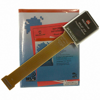
Manufacturer Part Number
PCM18XT0
Description
MODULE PROC PIC18F4685
Manufacturer
Microchip Technology
Datasheet
1.PCM18XT0.pdf
(484 pages)
Specifications of PCM18XT0
Accessory Type
Processor Module
Product
Microcontroller Modules
Core Processor
PIC18F4685
Lead Free Status / RoHS Status
Not applicable / Not applicable
For Use With/related Products
ICE2000
For Use With
ICE2000 - EMULATOR MPLAB-ICE 2000 POD
Lead Free Status / RoHS Status
Lead free / RoHS Compliant, Not applicable / Not applicable


PIC18F2682/2685/4682/4685
10.2
PORTB is an 8-bit wide, bidirectional port. The
corresponding data direction register is TRISB. Setting
a TRISB bit (= 1) will make the corresponding PORTB
pin an input (i.e., put the corresponding output driver in
a high-impedance mode). Clearing a TRISB bit (= 0)
will make the corresponding PORTB pin an output (i.e.,
put the contents of the output latch on the selected pin).
The Data Latch register (LATB) is also memory
mapped. Read-modify-write operations on the LATB
register read and write the latched output value for
PORTB.
Pins RB2 through RB3 are multiplexed with the ECAN
peripheral. Refer to Section 23.0 “ECAN™ Technol-
ogy” for proper settings of TRISB when CAN is
enabled.
EXAMPLE 10-2:
Each of the PORTB pins has a weak internal pull-up. A
single control bit can turn on all the pull-ups. This is
performed by clearing bit RBPU (INTCON2<7>). The
weak pull-up is automatically turned off when the port
pin is configured as an output. The pull-ups are
disabled on all device Resets.
DS39761C-page 134
CLRF
CLRF
MOVLW
MOVWF
MOVLW
MOVWF
PORTB, TRISB and LATB
Registers
PORTB
LATB
0Eh
ADCON1 ; digital I/O pins
0CFh
TRISB
; Initialize PORTB by
; clearing output
; data latches
; Alternate method
; to clear output
; data latches
; Set RB<4:0> as
; (required if config bit
; PBADEN is set)
; Value used to
; initialize data
; direction
; Set RB<3:0> as inputs
; RB<5:4> as outputs
; RB<7:6> as inputs
INITIALIZING PORTB
Four of the PORTB pins (RB7:RB4) have an
interrupt-on-change feature. Only pins configured as
inputs can cause this interrupt to occur (i.e., any
RB7:RB4 pin configured as an output is excluded
from the interrupt-on-change comparison). The input
pins (of RB7:RB4) are compared with the old value
latched on the last read of PORTB. The “mismatch”
outputs of RB7:RB4 are ORed together to generate
the RB Port Change Interrupt with Flag bit, RBIF
(INTCON<0>).
This interrupt can wake the device from Sleep. The
user, in the Interrupt Service Routine, can clear the
interrupt in the following manner:
a)
b)
A mismatch condition will continue to set flag bit, RBIF.
Reading PORTB will end the mismatch condition and
allow flag bit RBIF to be cleared.
The interrupt-on-change feature is recommended for
wake-up on key depression operation and operations
where PORTB is only used for the interrupt-on-change
feature. Polling of PORTB is not recommended while
using the interrupt-on-change feature.
Note:
Any read or write of PORTB (except with the
MOVFF (ANY), PORTB instruction). This will
end the mismatch condition.
Clear flag bit, RBIF.
On a Power-on Reset, RB4:RB0 are
configured as analog inputs by default and
read as ‘0’; RB7:RB5 are configured as
digital inputs.
By programming the Configuration bit,
PBADEN (CONFIG3H<1>), RB4:RB0 will
alternatively be configured as digital inputs
on POR.
© 2009 Microchip Technology Inc.
Related parts for PCM18XT0
Image
Part Number
Description
Manufacturer
Datasheet
Request
R

Part Number:
Description:
Manufacturer:
Microchip Technology Inc.
Datasheet:
Part Number:
Description:
Manufacturer:
Microchip Technology Inc.
Datasheet:
Part Number:
Description:
Manufacturer:
Microchip Technology Inc.
Datasheet:
Part Number:
Description:
Manufacturer:
Microchip Technology Inc.
Datasheet:
Part Number:
Description:
Manufacturer:
Microchip Technology Inc.
Datasheet:
Part Number:
Description:
Manufacturer:
Microchip Technology Inc.
Datasheet:
Part Number:
Description:
Manufacturer:
Microchip Technology Inc.
Datasheet:
Part Number:
Description:
Manufacturer:
Microchip Technology Inc.
Datasheet: