PCM18XT0 Microchip Technology, PCM18XT0 Datasheet - Page 475
PCM18XT0
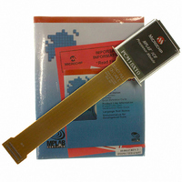
Manufacturer Part Number
PCM18XT0
Description
MODULE PROC PIC18F4685
Manufacturer
Microchip Technology
Datasheet
1.PCM18XT0.pdf
(484 pages)
Specifications of PCM18XT0
Accessory Type
Processor Module
Product
Microcontroller Modules
Core Processor
PIC18F4685
Lead Free Status / RoHS Status
Not applicable / Not applicable
For Use With/related Products
ICE2000
For Use With
ICE2000 - EMULATOR MPLAB-ICE 2000 POD
Lead Free Status / RoHS Status
Lead free / RoHS Compliant, Not applicable / Not applicable


Pinout I/O Descriptions
PIR Registers ................................................................... 120
PLL Frequency Multiplier ................................................... 27
PLL Lock Time-out ............................................................. 47
POP ................................................................................. 394
POR. See Power-on Reset.
PORTA
PORTB
PORTC
PORTD
PORTE
Postscaler, WDT
© 2009 Microchip Technology Inc.
RD0/PSP0/C1IN+ ...................................................... 22
RD1/PSP1/C1IN- ....................................................... 22
RD2/PSP2/C2IN+ ...................................................... 22
RD3/PSP3/C2IN- ....................................................... 22
RD4/PSP4/ECCP1/P1A ............................................. 22
RD5/PSP5/P1B .......................................................... 22
RD6/PSP6/P1C .......................................................... 22
RD7/PSP7/P1D .......................................................... 22
RE0/RD/AN5 .............................................................. 23
RE1/WR/AN6/C1OUT ................................................ 23
RE2/CS/AN7/C2OUT ................................................. 23
V
V
PIC18F2682/2685 ...................................................... 14
PIC18F4682/4685 ...................................................... 18
HSPLL Oscillator Mode .............................................. 27
INTOSC Modes .......................................................... 28
Use with INTOSC ....................................................... 27
Associated Registers ............................................... 133
I/O Summary ............................................................ 132
LATA Register .......................................................... 131
PORTA Register ...................................................... 131
TRISA Register ........................................................ 131
Associated Registers ............................................... 136
I/O Summary ............................................................ 135
LATB Register .......................................................... 134
PORTB Register ...................................................... 134
RB7:RB4 Interrupt-on-Change Flag (RBIF Bit) ........ 134
TRISB Register ........................................................ 134
Associated Registers ............................................... 139
I/O Summary ............................................................ 138
LATC Register ......................................................... 137
PORTC Register ...................................................... 137
RC3/SCK/SCL Pin ................................................... 203
TRISC Register ........................................................ 137
Associated Registers ............................................... 142
I/O Summary ............................................................ 141
LATD Register ......................................................... 140
Parallel Slave Port (PSP) Function .......................... 140
PORTD Register ...................................................... 140
TRISD Register ........................................................ 140
Associated Registers ............................................... 145
I/O Summary ............................................................ 145
LATE Register .......................................................... 143
PORTE Register ...................................................... 143
PSP Mode Select (PSPMODE Bit) .......................... 140
TRISE Register ........................................................ 143
Assignment (PSA Bit) .............................................. 151
Rate Select (T0PS2:T0PS0 Bits) ............................. 151
Switching Between Timer0 and WDT ...................... 151
DD
SS
....................................................................... 17, 23
...................................................................... 17, 23
PIC18F2682/2685/4682/4685
Power-Managed Modes ..................................................... 35
Power-on Reset (POR) ...................................................... 45
Power-up Delays ............................................................... 33
Power-up Timer (PWRT) ............................................. 33, 47
Prescaler
Prescaler, Timer0 ............................................................ 151
Prescaler, Timer2 ............................................................ 172
PRI_IDLE Mode ................................................................. 40
PRI_RUN Mode ................................................................. 36
Program Counter ............................................................... 64
Program Memory
Program Verification and Code Protection ...................... 360
Programming, Device Instructions ................................... 365
PSP. See Parallel Slave Port.
Pulse-Width Modulation. See PWM (CCP1/ECCP1 Modules).
PUSH ............................................................................... 394
PUSH and POP Instructions .............................................. 65
PUSHL ............................................................................. 410
PWM (CCP1 Module)
Clock Sources ........................................................... 35
Clock Transitions and Status Indicators .................... 36
Entering ..................................................................... 35
Exiting Idle and Sleep Modes .................................... 41
Idle Modes ................................................................. 39
Multiple Sleep Commands ......................................... 36
Run Modes ................................................................ 36
Selecting .................................................................... 35
Sleep Mode ............................................................... 39
Summary (table) ........................................................ 35
Power-up Timer (PWRT) ........................................... 47
Time-out Sequence ................................................... 47
Timer2 ..................................................................... 178
Assignment (PSA Bit) .............................................. 151
Rate Select (T0PS2:T0PS0 Bits) ............................. 151
Switching Between Timer0 and WDT ...................... 151
PCL, PCH and PCU Registers .................................. 64
PCLATH and PCLATU Registers .............................. 64
Code Protection ....................................................... 361
Extended Instruction Set ........................................... 93
Instructions ................................................................ 68
Interrupt Vector .......................................................... 63
Look-up Tables .......................................................... 66
Map and Stack (diagram) .......................................... 63
Reset Vector .............................................................. 63
Associated Registers ............................................... 361
Associated Registers ............................................... 173
CCPR1H:CCPR1L Registers .................................. 171
Duty Cycle ............................................................... 171
Example Frequencies/Resolutions .......................... 172
Period ...................................................................... 171
Setup for PWM Operation ....................................... 172
TMR2 to PR2 Match ................................................ 171
By Interrupt ........................................................ 41
By Reset ............................................................ 41
By WDT Time-out .............................................. 41
Without an Oscillator Start-up Delay ................. 42
PRI_IDLE .......................................................... 40
RC_IDLE ........................................................... 41
SEC_IDLE ......................................................... 40
PRI_RUN ........................................................... 36
RC_RUN ............................................................ 37
SEC_RUN ......................................................... 36
Two-Word .......................................................... 68
DS39761C-page 475
Related parts for PCM18XT0
Image
Part Number
Description
Manufacturer
Datasheet
Request
R

Part Number:
Description:
Manufacturer:
Microchip Technology Inc.
Datasheet:
Part Number:
Description:
Manufacturer:
Microchip Technology Inc.
Datasheet:
Part Number:
Description:
Manufacturer:
Microchip Technology Inc.
Datasheet:
Part Number:
Description:
Manufacturer:
Microchip Technology Inc.
Datasheet:
Part Number:
Description:
Manufacturer:
Microchip Technology Inc.
Datasheet:
Part Number:
Description:
Manufacturer:
Microchip Technology Inc.
Datasheet:
Part Number:
Description:
Manufacturer:
Microchip Technology Inc.
Datasheet:
Part Number:
Description:
Manufacturer:
Microchip Technology Inc.
Datasheet: