PCM18XT0 Microchip Technology, PCM18XT0 Datasheet - Page 251
PCM18XT0
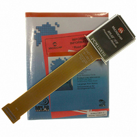
Manufacturer Part Number
PCM18XT0
Description
MODULE PROC PIC18F4685
Manufacturer
Microchip Technology
Datasheet
1.PCM18XT0.pdf
(484 pages)
Specifications of PCM18XT0
Accessory Type
Processor Module
Product
Microcontroller Modules
Core Processor
PIC18F4685
Lead Free Status / RoHS Status
Not applicable / Not applicable
For Use With/related Products
ICE2000
For Use With
ICE2000 - EMULATOR MPLAB-ICE 2000 POD
Lead Free Status / RoHS Status
Lead free / RoHS Compliant, Not applicable / Not applicable


REGISTER 19-3:
© 2009 Microchip Technology Inc.
bit 7
Legend:
R = Readable bit
-n = Value at POR
bit 7
bit 6
bit 5-3
bit 2-0
Note 1:
R/W-0
ADFM
If the A/D F
clock starts. This allows the SLEEP instruction to be executed before starting a conversion.
ADFM: A/D Result Format Select bit
1 = Right justified
0 = Left justified
Unimplemented: Read as ‘0’
ACQT2:ACQT0: A/D Acquisition Time Select bits
111 = 20 T
110 = 16 T
101 = 12 T
100 = 8 T
011 = 6 T
010 = 4 T
001 = 2 T
000 = 0 T
ADCS2:ADCS0: A/D Conversion Clock Select bits
111 = F
110 = F
101 = F
100 = F
011 = F
010 = F
001 = F
000 = F
U-0
—
ADCON2: A/D CONTROL REGISTER 2
RC
RC
OSC
OSC
OSC
RC
OSC
OSC
OSC
AD
AD
AD
AD
AD
clock source is selected, a delay of one T
AD
AD
AD
(clock derived from A/D RC oscillator)
(clock derived from A/D RC oscillator)
/64
/16
/4
/32
/8
/2
(1)
W = Writable bit
‘1’ = Bit is set
ACQT2
R/W-0
PIC18F2682/2685/4682/4685
ACQT1
R/W-0
U = Unimplemented bit, read as ‘0’
‘0’ = Bit is cleared
ACQT0
R/W-0
(1)
(1)
CY
(instruction cycle) is added before the A/D
ADCS2
R/W-0
x = Bit is unknown
ADCS1
R/W-0
DS39761C-page 251
ADCS0
R/W-0
bit 0
Related parts for PCM18XT0
Image
Part Number
Description
Manufacturer
Datasheet
Request
R

Part Number:
Description:
Manufacturer:
Microchip Technology Inc.
Datasheet:
Part Number:
Description:
Manufacturer:
Microchip Technology Inc.
Datasheet:
Part Number:
Description:
Manufacturer:
Microchip Technology Inc.
Datasheet:
Part Number:
Description:
Manufacturer:
Microchip Technology Inc.
Datasheet:
Part Number:
Description:
Manufacturer:
Microchip Technology Inc.
Datasheet:
Part Number:
Description:
Manufacturer:
Microchip Technology Inc.
Datasheet:
Part Number:
Description:
Manufacturer:
Microchip Technology Inc.
Datasheet:
Part Number:
Description:
Manufacturer:
Microchip Technology Inc.
Datasheet: