PCM18XT0 Microchip Technology, PCM18XT0 Datasheet - Page 253
PCM18XT0
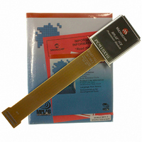
Manufacturer Part Number
PCM18XT0
Description
MODULE PROC PIC18F4685
Manufacturer
Microchip Technology
Datasheet
1.PCM18XT0.pdf
(484 pages)
Specifications of PCM18XT0
Accessory Type
Processor Module
Product
Microcontroller Modules
Core Processor
PIC18F4685
Lead Free Status / RoHS Status
Not applicable / Not applicable
For Use With/related Products
ICE2000
For Use With
ICE2000 - EMULATOR MPLAB-ICE 2000 POD
Lead Free Status / RoHS Status
Lead free / RoHS Compliant, Not applicable / Not applicable


The value in the ADRESH/ADRESL registers is not
modified for a Power-on Reset. The ADRESH/ADRESL
registers will contain unknown data after a Power-on
Reset.
After the A/D module has been configured as desired,
the selected channel must be acquired before the con-
version is started. The analog input channels must
have their corresponding TRIS bits selected as inputs.
To determine acquisition time, see Section 19.1 “A/D
Acquisition Requirements”. After this acquisition
time has elapsed, the A/D conversion can be started.
An acquisition time can be programmed to occur
between setting the GO/DONE bit and the actual start
of the conversion.
FIGURE 19-2:
© 2009 Microchip Technology Inc.
Legend: C
V
AIN
Rs
V
I
R
SS
C
R
LEAKAGE
PIN
T
IC
HOLD
SS
ANALOG INPUT MODEL
ANx
C
5 pF
PIN
= Input Capacitance
= Threshold Voltage
= Leakage Current at the pin due to
= Interconnect Resistance
= Sampling Switch
= Sample/Hold Capacitance (from DAC)
= Sampling Switch Resistance
various junctions
V
DD
PIC18F2682/2685/4682/4685
V
V
T
T
= 0.6V
= 0.6V
I
± 500 nA
LEAKAGE
The following steps should be followed to perform an
A/D conversion:
1.
2.
3.
4.
5.
6.
7.
R
IC
Configure the A/D module:
• Configure analog pins, voltage reference and
• Select A/D input channel (ADCON0)
• Select A/D acquisition time (ADCON2)
• Select A/D conversion clock (ADCON2)
• Turn on A/D module (ADCON0)
Configure A/D interrupt (if desired):
• Clear ADIF bit
• Set ADIE bit
• Set GIE bit
Wait the required acquisition time (if required).
Start conversion:
• Set GO/DONE bit (ADCON0 register)
Wait for A/D conversion to complete, by either:
• Polling for the GO/DONE bit to be cleared
OR
• Waiting for the A/D interrupt
Read A/D Result registers (ADRESH:ADRESL);
clear bit, ADIF, if required.
For next conversion, go to step 1 or step 2, as
required. The A/D conversion time per bit is
defined as T
required before next acquisition starts.
≤ 1k
digital I/O (ADCON1)
V
SS
DD
Sampling
Switch
6V
5V
4V
3V
2V
AD
R
SS
. A minimum wait of 2 T
Sampling Switch
5 6 7 8 9 10 11
V
SS
C
HOLD
DS39761C-page 253
= 120 pF
(kΩ)
AD
is
Related parts for PCM18XT0
Image
Part Number
Description
Manufacturer
Datasheet
Request
R

Part Number:
Description:
Manufacturer:
Microchip Technology Inc.
Datasheet:
Part Number:
Description:
Manufacturer:
Microchip Technology Inc.
Datasheet:
Part Number:
Description:
Manufacturer:
Microchip Technology Inc.
Datasheet:
Part Number:
Description:
Manufacturer:
Microchip Technology Inc.
Datasheet:
Part Number:
Description:
Manufacturer:
Microchip Technology Inc.
Datasheet:
Part Number:
Description:
Manufacturer:
Microchip Technology Inc.
Datasheet:
Part Number:
Description:
Manufacturer:
Microchip Technology Inc.
Datasheet:
Part Number:
Description:
Manufacturer:
Microchip Technology Inc.
Datasheet: