PCM18XT0 Microchip Technology, PCM18XT0 Datasheet - Page 336
PCM18XT0
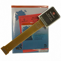
Manufacturer Part Number
PCM18XT0
Description
MODULE PROC PIC18F4685
Manufacturer
Microchip Technology
Datasheet
1.PCM18XT0.pdf
(484 pages)
Specifications of PCM18XT0
Accessory Type
Processor Module
Product
Microcontroller Modules
Core Processor
PIC18F4685
Lead Free Status / RoHS Status
Not applicable / Not applicable
For Use With/related Products
ICE2000
For Use With
ICE2000 - EMULATOR MPLAB-ICE 2000 POD
Lead Free Status / RoHS Status
Lead free / RoHS Compliant, Not applicable / Not applicable


PIC18F2682/2685/4682/4685
23.9.1
The microcontroller clock frequency generated from a
PLL circuit is subject to a jitter, also defined as Phase
Jitter or Phase Skew. For its PIC18 Enhanced micro-
controllers, Microchip specifies phase jitter (P
being 2% (Gaussian distribution, within 3 standard
deviations, see parameter F13 in Table 27-7) and Total
Jitter (T
FIGURE 23-5:
Once these considerations are taken into account, it is
possible to show that the relation between the jitter and
the total frequency error can be defined as:
EQUATION 23-4:
where jitter is expressed in terms of time and NBT is the
Nominal Bit Time.
DS39761C-page 336
jitter
Nominal Clock
Clock with Jitter
CAN bit Time
with Jitter
) as being 2 * P
EXTERNAL CLOCK, INTERNAL
CLOCK AND MEASURABLE JITTER
IN HSPLL-BASED OSCILLATORS
Δf
=
----------------------- -
10 NBT
T
EFFECTS OF PHASE JITTER ON THE MICROCONTROLLER CLOCK
AND CAN BIT TIME
×
jitter
jitter
=
.
----------------------- -
10 NBT
2 P
×
×
jitter
jitter
) as
Phase Skew (Jitter)
CAN bit Jitter
The CAN protocol uses a bit-stuffing technique that
inserts a bit of a given polarity following five bits with the
opposite polarity. This gives a total of 10 bits transmit-
ted without re-synchronization (compensation for jitter
or phase error).
Given the random nature of the jitter error added, it can
be shown that the total error caused by the jitter tends
to cancel itself over time. For a period of 10 bits, it is
necessary to add only two jitter intervals to correct for
jitter-induced error: one interval in the beginning of the
10-bit period and another at the end. The overall effect
is shown in Figure 23-5.
For example, assume a CAN bit rate of 125 Kb/s, which
gives an NBT of 8 μs. For a 16 MHz clock generated
from a 4x PLL, the jitter at this clock frequency is:
EQUATION 23-5:
The resultant frequency error is:
EQUATION 23-6:
2
-------------------------------------- -
10
×
2%
(
×
1.25
(
8
×
×10
-------------------
16 MHz
×10
–
1
–
6
9
)
)
=
© 2009 Microchip Technology Inc.
=
3.125
-----------------
16
0.02
×10
×10
6
5 –
=
=
1.25ns
0.0031%
Related parts for PCM18XT0
Image
Part Number
Description
Manufacturer
Datasheet
Request
R

Part Number:
Description:
Manufacturer:
Microchip Technology Inc.
Datasheet:
Part Number:
Description:
Manufacturer:
Microchip Technology Inc.
Datasheet:
Part Number:
Description:
Manufacturer:
Microchip Technology Inc.
Datasheet:
Part Number:
Description:
Manufacturer:
Microchip Technology Inc.
Datasheet:
Part Number:
Description:
Manufacturer:
Microchip Technology Inc.
Datasheet:
Part Number:
Description:
Manufacturer:
Microchip Technology Inc.
Datasheet:
Part Number:
Description:
Manufacturer:
Microchip Technology Inc.
Datasheet:
Part Number:
Description:
Manufacturer:
Microchip Technology Inc.
Datasheet: