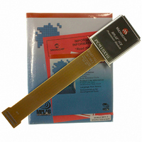
PCM18XT0 Microchip Technology, PCM18XT0 Datasheet - Page 265

PCM18XT0
Manufacturer Part Number
PCM18XT0
Description
MODULE PROC PIC18F4685
Manufacturer
Microchip Technology
Datasheet
1.PCM18XT0.pdf
(484 pages)
Specifications of PCM18XT0
Accessory Type
Processor Module
Product
Microcontroller Modules
Core Processor
PIC18F4685
Lead Free Status / RoHS Status
Not applicable / Not applicable
For Use With/related Products
ICE2000
For Use With
ICE2000 - EMULATOR MPLAB-ICE 2000 POD
Lead Free Status / RoHS Status
Lead free / RoHS Compliant, Not applicable / Not applicable
- Current page: 265 of 484
- Download datasheet (9Mb)
21.0
The comparator voltage reference is a 16-tap resistor
ladder network that provides a selectable reference
voltage. Although its primary purpose is to provide a
reference for the analog comparators, it may also be
used independently of them.
A block diagram is of the module shown in Figure 21-1.
The resistor ladder is segmented to provide two ranges
of CV
conserve power when the reference is not being used.
The module’s supply reference can be provided from
either device V
21.1
The voltage reference module is controlled through the
CVRCON register (Register 21-1). The comparator
voltage reference provides two ranges of output
REGISTER 21-1:
© 2009 Microchip Technology Inc.
bit 7
Legend:
R = Readable bit
-n = Value at POR
bit 7
bit 6
bit 5
bit 4
bit 3-0
Note 1:
Note:
CVREN
R/W-0
REF
COMPARATOR VOLTAGE
REFERENCE MODULE
Configuring the Comparator
Voltage Reference
values and has a power-down function to
CVROE overrides the TRISA<0> bit setting. If enabled for output, RA2 must also be configured as an
input by setting TRISA<2> to ‘1’.
Comparators are only available in 40/44-pin
devices (PIC18F4682/4685).
DD
CVREN: Comparator Voltage Reference Enable bit
1 = CV
0 = CV
CVROE: Comparator V
1 = CV
0 = CV
CVRR: Comparator V
1 = 0.00 CV
0 = 0.25 CV
CVRSS: Comparator V
1 = Comparator reference source, CV
0 = Comparator reference source, CV
CVR3:CVR0: Comparator V
When CVRR = 1:
CV
When CVRR = 0:
CV
/V
CVROE
SS
REF
REF
R/W-0
or an external voltage reference.
CVRCON: COMPARATOR VOLTAGE REFERENCE CONTROL REGISTER
= ((CVR3:CVR0)/24) • (CV
= (CV
REF
REF
REF
REF
(1)
circuit powered on
circuit powered down
voltage level is also output on the RA0/AN0/CV
voltage is disconnected from the RA0/AN0/CV
RSRC
RSRC
RSRC
W = Writable bit
‘1’ = Bit is set
to 0.75 CV
to 0.75 CV
R/W-0
CVRR
/4) + ((CVR3:CVR0)/32) • (CV
REF
REF
REF
Range Selection bit
Source Selection bit
Output Enable bit
REF
RSRC
RSRC
PIC18F2682/2685/4682/4685
CVRSS
R/W-0
Value Selection bits (0 ≤ (CVR3:CVR0) ≤ 15)
, with CV
, with CV
RSRC
RSRC
RSRC
)
RSRC
RSRC
U = Unimplemented bit, read as ‘0’
‘0’ = Bit is cleared
= (V
= V
(1)
R/W-0
CVR3
voltage, each with 16 distinct levels. The range to be
used is selected by the CVRR bit (CVRCON<5>). The
primary difference between the ranges is the size of the
steps
(CVR3:CVR0), with one range offering finer resolution.
The equations used to calculate the output of the
comparator voltage reference are as follows:
The comparator reference supply voltage can come
from either V
V
voltage source is selected by the CVRSS bit
(CVRCON<4>).
The settling time of the comparator voltage reference
must be considered when changing the CV
(see
Characteristics”).
/24 step size
/32 step size
DD
REF
REF
RSRC
– V
If CVRR = 1:
CV
If CVRR = 0:
CV
CV
- that are multiplexed with RA2 and RA3. The
+) – (V
)
SS
REF
REF
RSRC
Table 27-3
selected
REF
= ((CVR3:CVR0)/24) x CV
REF
= (CV
REF
)
DD
R/W-0
CVR2
pin
-)
pin
and V
DD
by
x 1/4) + (((CVR3:CVR0)/32) x
in
SS
the
, or the external V
x = Bit is unknown
Section 27.0
R/W-0
CVR1
CV
REF
DS39761C-page 265
RSRC
selection
“Electrical
REF
R/W-0
CVR0
REF
output
+ and
bit 0
bits
Related parts for PCM18XT0
Image
Part Number
Description
Manufacturer
Datasheet
Request
R

Part Number:
Description:
Manufacturer:
Microchip Technology Inc.
Datasheet:

Part Number:
Description:
Manufacturer:
Microchip Technology Inc.
Datasheet:

Part Number:
Description:
Manufacturer:
Microchip Technology Inc.
Datasheet:

Part Number:
Description:
Manufacturer:
Microchip Technology Inc.
Datasheet:

Part Number:
Description:
Manufacturer:
Microchip Technology Inc.
Datasheet:

Part Number:
Description:
Manufacturer:
Microchip Technology Inc.
Datasheet:

Part Number:
Description:
Manufacturer:
Microchip Technology Inc.
Datasheet:

Part Number:
Description:
Manufacturer:
Microchip Technology Inc.
Datasheet:


