PCM18XT0 Microchip Technology, PCM18XT0 Datasheet - Page 472
PCM18XT0
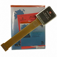
Manufacturer Part Number
PCM18XT0
Description
MODULE PROC PIC18F4685
Manufacturer
Microchip Technology
Datasheet
1.PCM18XT0.pdf
(484 pages)
Specifications of PCM18XT0
Accessory Type
Processor Module
Product
Microcontroller Modules
Core Processor
PIC18F4685
Lead Free Status / RoHS Status
Not applicable / Not applicable
For Use With/related Products
ICE2000
For Use With
ICE2000 - EMULATOR MPLAB-ICE 2000 POD
Lead Free Status / RoHS Status
Lead free / RoHS Compliant, Not applicable / Not applicable


PIC18F2682/2685/4682/4685
Enhanced Capture/Compare/PWM (ECCP1) .................. 175
Enhanced Universal Synchronous Receiver Transmitter (EU-
Equations
Errata ................................................................................... 7
Error Recognition Mode ................................................... 327
EUSART
Extended Instruction Set
External Clock Input ........................................................... 26
F
Fail-Safe Clock Monitor ............................................ 345, 358
DS39761C-page 472
Associated Registers ............................................... 188
Capture and Compare Modes .................................. 176
Capture Mode. See Capture (ECCP1 Module).
Outputs and Configuration ....................................... 176
Pin Configurations for ECCP1 ................................. 176
PWM Mode. See PWM (ECCP1 Module).
Standard PWM Mode ............................................... 176
Timer Resources ...................................................... 176
SART). See EUSART.
A/D Acquisition Time ................................................ 254
A/D Minimum Charging Time ................................... 254
Calculating the Minimum Required A/D Acquisition Time
Asynchronous Mode ................................................ 238
Baud Rate Generator (BRG) .................................... 233
Synchronous Master Mode ...................................... 244
Synchronous Slave Mode ........................................ 247
ADDFSR .................................................................. 408
ADDULNK ................................................................ 408
CALLW ..................................................................... 409
MOVSF .................................................................... 409
MOVSS .................................................................... 410
PUSHL ..................................................................... 410
SUBFSR .................................................................. 411
SUBULNK ................................................................ 411
Exiting Operation ..................................................... 358
Interrupts in Power-Managed Modes ....................... 359
POR or Wake-up from Sleep ................................... 359
Watchdog Timer (WDT) ........................................... 358
Associated Registers, Receive ........................ 241
Associated Registers, Transmit ....................... 239
Auto-Wake-up on Sync Break Character ......... 242
Break Character Sequence .............................. 243
Receiver ........................................................... 240
Receiving a Break Character ........................... 243
Setting Up 9-Bit Mode with
Transmitter ....................................................... 238
Associated Registers ....................................... 233
Auto-Baud Rate Detect .................................... 236
Baud Rate Error, Calculating ........................... 233
Baud Rates, Asynchronous Modes .................. 234
High Baud Rate Select (BRGH Bit) .................. 233
Operation in Power-Managed Modes .............. 233
Sampling .......................................................... 233
Associated Registers, Receive ........................ 246
Associated Registers, Transmit ....................... 245
Reception ......................................................... 246
Transmission .................................................... 244
Associated Registers, Receive ........................ 248
Associated Registers, Transmit ....................... 247
Reception ......................................................... 248
Transmission .................................................... 247
.......................................................................... 254
Address Detect ........................................ 240
Fast Register Stack ........................................................... 66
Firmware Instructions ...................................................... 365
Flash Program Memory ..................................................... 97
FSCM. See Fail-Safe Clock Monitor.
G
GOTO .............................................................................. 386
H
Hardware Multiplier .......................................................... 113
High/Low-Voltage Detect ................................................. 269
HLVD. See High/Low-Voltage Detect. ............................. 269
I
I/O Ports ........................................................................... 131
I
2
C Mode (MSSP)
Associated Registers ............................................... 105
Control Registers ....................................................... 98
Erase Sequence ...................................................... 102
Erasing .................................................................... 102
Operation During Code-Protect ............................... 105
Reading ................................................................... 101
Table Pointer
Table Pointer Boundaries ........................................ 100
Table Pointer Operations (table) .............................. 100
Table Reads and Table Writes .................................. 97
Write Sequence ....................................................... 103
Write Verify .............................................................. 105
Writing ..................................................................... 103
Introduction .............................................................. 113
Operation ................................................................. 113
Performance Comparison ........................................ 113
Associated Registers ............................................... 273
Characteristics ......................................................... 434
Current Consumption ............................................... 271
Effects of a Reset .................................................... 273
Operation ................................................................. 270
Operation During Sleep ........................................... 273
Setup ....................................................................... 271
Start-up Time ........................................................... 271
Typical Application ................................................... 272
Acknowledge Sequence Timing .............................. 222
Baud Rate Generator .............................................. 215
Bus Collision
Clock Arbitration ...................................................... 216
Clock Stretching ....................................................... 208
Clock Synchronization and the CKP Bit ................... 209
Effect of a Reset ...................................................... 223
General Call Address Support ................................. 212
I
2
C Clock Rate w/BRG ............................................. 215
EECON1 ............................................................ 98
EECON2 ............................................................ 98
TABLAT ............................................................. 98
TABLAT (Table Latch) Register ...................... 100
TBLPTR ............................................................. 98
TBLPTR (Table Pointer) Register .................... 100
Boundaries Based on Operation ..................... 100
Protection Against Spurious Writes ................. 105
Unexpected Termination ................................. 105
During a Repeated Start Condition .................. 226
During a Start Condition .................................. 224
During a Stop Condition .................................. 227
10-Bit Slave Receive Mode (SEN = 1) ............ 208
10-Bit Slave Transmit Mode ............................ 208
7-Bit Slave Receive Mode (SEN = 1) .............. 208
7-Bit Slave Transmit Mode .............................. 208
© 2009 Microchip Technology Inc.
Related parts for PCM18XT0
Image
Part Number
Description
Manufacturer
Datasheet
Request
R

Part Number:
Description:
Manufacturer:
Microchip Technology Inc.
Datasheet:
Part Number:
Description:
Manufacturer:
Microchip Technology Inc.
Datasheet:
Part Number:
Description:
Manufacturer:
Microchip Technology Inc.
Datasheet:
Part Number:
Description:
Manufacturer:
Microchip Technology Inc.
Datasheet:
Part Number:
Description:
Manufacturer:
Microchip Technology Inc.
Datasheet:
Part Number:
Description:
Manufacturer:
Microchip Technology Inc.
Datasheet:
Part Number:
Description:
Manufacturer:
Microchip Technology Inc.
Datasheet:
Part Number:
Description:
Manufacturer:
Microchip Technology Inc.
Datasheet: