PCM18XT0 Microchip Technology, PCM18XT0 Datasheet - Page 180
PCM18XT0
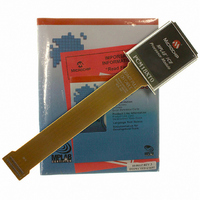
Manufacturer Part Number
PCM18XT0
Description
MODULE PROC PIC18F4685
Manufacturer
Microchip Technology
Datasheet
1.PCM18XT0.pdf
(484 pages)
Specifications of PCM18XT0
Accessory Type
Processor Module
Product
Microcontroller Modules
Core Processor
PIC18F4685
Lead Free Status / RoHS Status
Not applicable / Not applicable
For Use With/related Products
ICE2000
For Use With
ICE2000 - EMULATOR MPLAB-ICE 2000 POD
Lead Free Status / RoHS Status
Lead free / RoHS Compliant, Not applicable / Not applicable


PIC18F2682/2685/4682/4685
16.4.4
In the Half-Bridge Output mode, two pins are used as
outputs to drive push-pull loads. The PWM output
signal is output on the P1A pin, while the complemen-
tary PWM output signal is output on the P1B pin
(Figure 16-4). This mode can be used for half-bridge
applications, as shown in Figure 16-5, or for full-bridge
applications where four power switches are being
modulated with two PWM signals.
In Half-Bridge Output mode, the programmable dead-
band delay can be used to prevent shoot-through
current in half-bridge power devices. The value of bits,
PDC6:PDC0, sets the number of instruction cycles
before the output is driven active. If the value is greater
than the duty cycle, the corresponding output remains
inactive during the entire cycle. See Section 16.4.6
“Programmable Dead-Band Delay” for more details
of the dead-band delay operations.
Since the P1A and P1B outputs are multiplexed with
the PORTD<4> and PORTD<5> data latches, the
TRISD<4> and TRISD<5> bits must be cleared to
configure P1A and P1B as outputs.
FIGURE 16-5:
DS39761C-page 180
HALF-BRIDGE MODE
Standard Half-Bridge Circuit (“Push-Pull”)
Half-Bridge Output Driving a Full-Bridge Circuit
EXAMPLES OF HALF-BRIDGE OUTPUT MODE APPLICATIONS
PIC18F268X/468X
P1A
P1B
PIC18F268X/468X
P1A
P1B
FET
Driver
FET
Driver
FET
Driver
FET
Driver
FIGURE 16-4:
Note 1: At this time, the TMR2 register is equal to the
P1A
P1B
td = Dead-Band Delay
(2)
(2)
2: Output signals are shown as active-high.
Load
V+
V-
(1)
PR2 register.
V+
V-
Duty Cycle
td
Period
Load
td
HALF-BRIDGE PWM
OUTPUT
© 2009 Microchip Technology Inc.
FET
Driver
FET
Driver
(1)
+
V
-
+
V
-
Period
(1)
Related parts for PCM18XT0
Image
Part Number
Description
Manufacturer
Datasheet
Request
R

Part Number:
Description:
Manufacturer:
Microchip Technology Inc.
Datasheet:
Part Number:
Description:
Manufacturer:
Microchip Technology Inc.
Datasheet:
Part Number:
Description:
Manufacturer:
Microchip Technology Inc.
Datasheet:
Part Number:
Description:
Manufacturer:
Microchip Technology Inc.
Datasheet:
Part Number:
Description:
Manufacturer:
Microchip Technology Inc.
Datasheet:
Part Number:
Description:
Manufacturer:
Microchip Technology Inc.
Datasheet:
Part Number:
Description:
Manufacturer:
Microchip Technology Inc.
Datasheet:
Part Number:
Description:
Manufacturer:
Microchip Technology Inc.
Datasheet: