PCM18XT0 Microchip Technology, PCM18XT0 Datasheet - Page 260
PCM18XT0
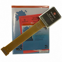
Manufacturer Part Number
PCM18XT0
Description
MODULE PROC PIC18F4685
Manufacturer
Microchip Technology
Datasheet
1.PCM18XT0.pdf
(484 pages)
Specifications of PCM18XT0
Accessory Type
Processor Module
Product
Microcontroller Modules
Core Processor
PIC18F4685
Lead Free Status / RoHS Status
Not applicable / Not applicable
For Use With/related Products
ICE2000
For Use With
ICE2000 - EMULATOR MPLAB-ICE 2000 POD
Lead Free Status / RoHS Status
Lead free / RoHS Compliant, Not applicable / Not applicable


PIC18F2682/2685/4682/4685
20.1
There are eight modes of operation for the compara-
tors, shown in Figure 20-1. Bits CM2:CM0 of the
CMCON register are used to select these modes. The
TRISA register controls the data direction of the com-
parator pins for each mode. If the Comparator mode is
FIGURE 20-1:
DS39761C-page 260
Comparators Reset (POR Default Value)
CM2:CM0 = 000
Two Independent Comparators
CM2:CM0 = 010
Two Common Reference Comparators
CM2:CM0 = 100
One Independent Comparator with Output
CM2:CM0 = 001
RD1/PSP1/C1IN-
RD0/PSP0/C1IN+
RD3/PSP3/C2IN-
RD2/PSP2/C2IN+
RD1/PSP1/C1IN-
RD0/PSP0/C1IN+
RD3/PSP3/C2IN-
RD2/PSP2/C2IN+
RD1/PSP1/C1IN-
RD0/PSP0/C1IN+
RD3/PSP3/C2IN-
RD2/PSP2/C2IN+
A = Analog Input, port reads zeros always
* Setting the TRISA<5:4> bits will disable the comparator outputs by configuring the pins as inputs.
RD1/PSP1/C1IN-
RD0/PSP0/C1IN+
RE1/WR/AN6/C1OUT*
RD3/PSP3/C2IN-
RD2/PSP2/C2IN+
Comparator Configuration
A
A
A
D
A
A
A
A
A
A
A
A
COMPARATOR I/O OPERATING MODES
A
A
D
D
V
V
V
V
V
V
V
V
V
V
V
V
IN
IN
IN
IN
V
V
V
V
IN
IN
IN
IN
IN
IN
IN
IN
-
+
-
+
IN
IN
IN
IN
-
+
-
+
-
+
-
+
-
+
-
+
C1
C2
C1
C2
C1
C2
C1
C2
C1OUT
C2OUT
D = Digital Input
Off
Off
(Read as ‘0’)
C1OUT
C2OUT
(Read as ‘0’)
C1OUT
Off
(Read as ‘0’)
Two Common Reference Comparators with Outputs
CM2:CM0 = 101
Two Independent Comparators with Outputs
CM2:CM0 = 011
Comparators Off
CM2:CM0 = 111
Four Inputs Multiplexed to Two Comparators
CM2:CM0 = 110
RD1/PSP1/
C1IN-
RD0/PSP0/
C1IN+
RD3/PSP3/
C2IN-
RD2/PSP2/
C2IN+
RD1/PSP1/C1IN-
RD0/PSP0/C1IN+
RD3/PSP3/C2IN-
RD2/PSP2/C2IN+
RD1/PSP1/C1IN-
RD0/PSP0/C1IN+
RE1/WR/AN6/C1OUT*
RD3/PSP3/C2IN-
RD2/PSP2/C2IN+
RE2/CS/AN7/C2OUT*
RD1/PSP1/C1IN-
RD0/PSP0/C1IN+
RE1/WR/AN6/C1OUT*
RD3/PSP3/C2IN-
RD2/PSP2/C2IN+
RE2/CS/AN7/C2OUT*
changed, the comparator output level may not be valid
for the specified mode change delay shown in
Section 27.0 “Electrical Characteristics”.
Note:
CIS (CMCON<3>) is the Comparator Input Switch
A
A
A
A
Comparator interrupts should be disabled
during a Comparator mode change;
otherwise, a false interrupt may occur.
CIS = 0
CIS = 1
CIS = 0
CIS = 1
A
A
A
D
A
A
A
A
D
D
D
D
© 2009 Microchip Technology Inc.
V
V
V
V
V
V
V
V
V
V
V
V
IN
IN
IN
IN
IN
IN
IN
IN
IN
IN
IN
IN
-
+
-
+
-
+
-
+
V
V
V
V
-
+
-
+
IN
IN
IN
IN
CV
-
+
-
+
C1
C2
C1
C2
C1
C2
REF
C1
C2
From V
C1OUT
C2OUT
C1OUT
C2OUT
Off
(Read as ‘0’)
Off
(Read as ‘0’)
REF
C1OUT
C2OUT
Module
Related parts for PCM18XT0
Image
Part Number
Description
Manufacturer
Datasheet
Request
R

Part Number:
Description:
Manufacturer:
Microchip Technology Inc.
Datasheet:
Part Number:
Description:
Manufacturer:
Microchip Technology Inc.
Datasheet:
Part Number:
Description:
Manufacturer:
Microchip Technology Inc.
Datasheet:
Part Number:
Description:
Manufacturer:
Microchip Technology Inc.
Datasheet:
Part Number:
Description:
Manufacturer:
Microchip Technology Inc.
Datasheet:
Part Number:
Description:
Manufacturer:
Microchip Technology Inc.
Datasheet:
Part Number:
Description:
Manufacturer:
Microchip Technology Inc.
Datasheet:
Part Number:
Description:
Manufacturer:
Microchip Technology Inc.
Datasheet: