PCM18XT0 Microchip Technology, PCM18XT0 Datasheet - Page 145
PCM18XT0
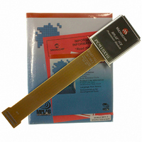
Manufacturer Part Number
PCM18XT0
Description
MODULE PROC PIC18F4685
Manufacturer
Microchip Technology
Datasheet
1.PCM18XT0.pdf
(484 pages)
Specifications of PCM18XT0
Accessory Type
Processor Module
Product
Microcontroller Modules
Core Processor
PIC18F4685
Lead Free Status / RoHS Status
Not applicable / Not applicable
For Use With/related Products
ICE2000
For Use With
ICE2000 - EMULATOR MPLAB-ICE 2000 POD
Lead Free Status / RoHS Status
Lead free / RoHS Compliant, Not applicable / Not applicable


TABLE 10-9:
TABLE 10-10: SUMMARY OF REGISTERS ASSOCIATED WITH PORTE
© 2009 Microchip Technology Inc.
PORTE
LATE
TRISE
ADCON1
CMCON
Legend: — = unimplemented, read as ‘0’. Shaded cells are not used by PORTE.
Note 1:
RE0/RD/AN5
RE1/WR/AN6/C1OUT RE1
RE2/CS/AN7/C2OUT
MCLR/V
Legend:
Name
(3)
Pin Name
2:
3:
(3)
(3)
PP
(3)
/RE3
Implemented only when Master Clear functionality is disabled (MCLRE Configuration bit = 0).
RE3 is the only PORTE bit implemented on both PIC18F2682/2685 and PIC18F4682/4685 devices. All
other bits are implemented only when PORTE is implemented (i.e., PIC18F4682/4685 devices).
These registers are unimplemented on PIC18F2682/2685 devices.
OUT = Output; IN = Input; ANA = Analog Signal; DIG = Digital Output; ST = Schmitt Buffer Input; TTL = TTL Buffer Input
C2OUT
Bit 7
IBF
—
—
—
PORTE I/O SUMMARY
RE0
RE2
Function
RD
AN5
WR
AN6
C1OUT
CS
AN7
C2OUT
MCLR
V
RE3
PP
C1OUT
Bit 6
OBF
—
—
—
OUT
OUT
OUT
OUT
OUT
I/O
IN
IN
IN
IN
IN
IN
IN
IN
IN
IN
IN
IN
TRIS Buffer
VCFG1
C2INV
IBOV
Bit 5
0
1
1
1
0
1
1
1
0
0
1
1
1
0
x
x
1
—
—
PIC18F2682/2685/4682/4685
ANA
ANA
ANA
ANA
DIG
TTL
DIG
TTL
DIG
DIG
TTL
DIG
ST
ST
ST
ST
ST
PSPMODE
VCFG0
C1INV
Bit 4
Comparator 1 output.
Comparator 2 output.
LATE<0> data output.
PORTE<0> data input.
PSP read enable input.
A/D input channel 5. Enabled on POR, this analog input overrides the
digital input (read as clear – low level).
LATE<1> data output.
PORTE<1> data input.
PSP write enable input.
A/D input channel 6. Enabled on POR, this analog input overrides the
digital input (read as clear – low level).
LATE<2> data output.
PORTE<2> data input.
PSP chip select input.
A/D input channel 7. Enabled on POR, this analog input overrides the
digital input (read as clear – low level).
External Reset input. Disabled when MCLRE Configuration bit is ‘1’.
High-voltage detection; used by ICSP™ operation.
PORTE<3> data input. Disabled when MCLRE Configuration bit is ‘0’.
—
—
RE3
PCFG3
Bit 3
CIS
—
—
(1,2)
LATE Data Output Register
TRISE2
PCFG2
Bit 2
CM2
RE2
Description
TRISE1
PCFG1
Bit 1
CM1
RE1
TRISE0
PCFG0
Bit 0
DS39761C-page 145
CM0
RE0
on page
Values
Reset
54
54
54
52
53
Related parts for PCM18XT0
Image
Part Number
Description
Manufacturer
Datasheet
Request
R

Part Number:
Description:
Manufacturer:
Microchip Technology Inc.
Datasheet:
Part Number:
Description:
Manufacturer:
Microchip Technology Inc.
Datasheet:
Part Number:
Description:
Manufacturer:
Microchip Technology Inc.
Datasheet:
Part Number:
Description:
Manufacturer:
Microchip Technology Inc.
Datasheet:
Part Number:
Description:
Manufacturer:
Microchip Technology Inc.
Datasheet:
Part Number:
Description:
Manufacturer:
Microchip Technology Inc.
Datasheet:
Part Number:
Description:
Manufacturer:
Microchip Technology Inc.
Datasheet:
Part Number:
Description:
Manufacturer:
Microchip Technology Inc.
Datasheet: