PCM18XT0 Microchip Technology, PCM18XT0 Datasheet - Page 190
PCM18XT0
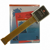
Manufacturer Part Number
PCM18XT0
Description
MODULE PROC PIC18F4685
Manufacturer
Microchip Technology
Datasheet
1.PCM18XT0.pdf
(484 pages)
Specifications of PCM18XT0
Accessory Type
Processor Module
Product
Microcontroller Modules
Core Processor
PIC18F4685
Lead Free Status / RoHS Status
Not applicable / Not applicable
For Use With/related Products
ICE2000
For Use With
ICE2000 - EMULATOR MPLAB-ICE 2000 POD
Lead Free Status / RoHS Status
Lead free / RoHS Compliant, Not applicable / Not applicable


PIC18F2682/2685/4682/4685
17.3.1
The MSSP module has four registers for SPI mode
operation. These are:
• MSSP Control Register 1 (SSPCON1)
• MSSP Status Register (SSPSTAT)
• Serial Receive/Transmit Buffer Register
• MSSP Shift Register (SSPSR) – Not directly
SSPCON1 and SSPSTAT are the control and status
registers in SPI mode operation. The SSPCON1
register is readable and writable. The lower 6 bits of
the SSPSTAT are read-only. The upper two bits of the
SSPSTAT are read/write.
REGISTER 17-1:
DS39761C-page 190
bit 7
Legend:
R = Readable bit
-n = Value at POR
bit 7
bit 6
bit 5
bit 4
bit 3
bit 2
bit 1
bit 0
(SSPBUF)
accessible
R/W-0
SMP
REGISTERS
SMP: Sample bit
SPI Master mode:
1 = Input data sampled at end of data output time
0 = Input data sampled at middle of data output time
SPI Slave mode:
SMP must be cleared when SPI is used in Slave mode.
CKE: SPI Clock Select bit
1 = Transmit occurs on transition from active to Idle clock state
0 = Transmit occurs on transition from Idle to active clock state
Polarity of clock state is set by the CKP bit (SSPCON1<4>).
D/A: Data/Address bit
Used in I
P: Stop bit
Used in I
S: Start bit
Used in I
R/W: Read/Write Information bit
Used in I
UA: Update Address bit
Used in I
BF: Buffer Full Status bit (Receive mode only)
1 = Receive complete, SSPBUF is full
0 = Receive not complete, SSPBUF is empty
R/W-0
CKE
SSPSTAT: MSSP STATUS REGISTER (SPI MODE)
2
2
2
2
2
C mode only.
C mode only. This bit is cleared when the MSSP module is disabled, SSPEN is cleared.
C mode only.
C mode only.
C mode only.
W = Writable bit
‘1’ = Bit is set
D/A
R-0
R-0
P
U = Unimplemented bit, read as ‘0’
‘0’ = Bit is cleared
SSPSR is the shift register used for shifting data in or
out. SSPBUF is the buffer register to which data bytes
are written to or read from.
In receive operations, SSPSR and SSPBUF together
create a double-buffered receiver. When SSPSR
receives a complete byte, it is transferred to SSPBUF
and the SSPIF interrupt is set.
During transmission, the SSPBUF is not double-
buffered. A write to SSPBUF will write to both SSPBUF
and SSPSR.
R-0
S
R/W
R-0
© 2009 Microchip Technology Inc.
x = Bit is unknown
R-0
UA
R-0
BF
bit 0
Related parts for PCM18XT0
Image
Part Number
Description
Manufacturer
Datasheet
Request
R

Part Number:
Description:
Manufacturer:
Microchip Technology Inc.
Datasheet:
Part Number:
Description:
Manufacturer:
Microchip Technology Inc.
Datasheet:
Part Number:
Description:
Manufacturer:
Microchip Technology Inc.
Datasheet:
Part Number:
Description:
Manufacturer:
Microchip Technology Inc.
Datasheet:
Part Number:
Description:
Manufacturer:
Microchip Technology Inc.
Datasheet:
Part Number:
Description:
Manufacturer:
Microchip Technology Inc.
Datasheet:
Part Number:
Description:
Manufacturer:
Microchip Technology Inc.
Datasheet:
Part Number:
Description:
Manufacturer:
Microchip Technology Inc.
Datasheet: