PCM18XT0 Microchip Technology, PCM18XT0 Datasheet - Page 398
PCM18XT0
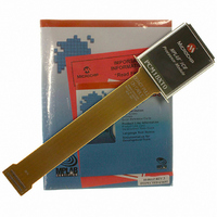
Manufacturer Part Number
PCM18XT0
Description
MODULE PROC PIC18F4685
Manufacturer
Microchip Technology
Datasheet
1.PCM18XT0.pdf
(484 pages)
Specifications of PCM18XT0
Accessory Type
Processor Module
Product
Microcontroller Modules
Core Processor
PIC18F4685
Lead Free Status / RoHS Status
Not applicable / Not applicable
For Use With/related Products
ICE2000
For Use With
ICE2000 - EMULATOR MPLAB-ICE 2000 POD
Lead Free Status / RoHS Status
Lead free / RoHS Compliant, Not applicable / Not applicable


PIC18F2682/2685/4682/4685
RLNCF
Syntax:
Operands:
Operation:
Status Affected:
Encoding:
Description:
Words:
Cycles:
Example:
DS39761C-page 398
Q Cycle Activity:
Before Instruction
After Instruction
Decode
REG
REG
Q1
=
=
register ‘f’
Rotate Left f (No Carry)
0 ≤ f ≤ 255
d ∈ [0,1]
a ∈ [0,1]
(f<n>) → dest<n + 1>,
(f<7>) → dest<0>
N, Z
The contents of register ‘f’ are rotated
one bit to the left. If ‘d’ is ‘0’, the result
is placed in W. If ‘d’ is ‘1’, the result is
stored back in register ‘f’ (default).
If ‘a’ is ‘0’, the Access Bank is selected.
If ‘a’ is ‘1’, the BSR is used to select the
GPR bank (default).
If ‘a’ is ‘0’ and the extended instruction
set is enabled, this instruction operates
in Indexed Literal Offset Addressing
mode whenever f ≤ 95 (5Fh). See
Section 25.2.3 “Byte-Oriented and
Bit-Oriented Instructions in Indexed
Literal Offset Mode” for details.
1
1
RLNCF
RLNCF
Read
Q2
0100
1010 1011
0101 0111
f {,d {,a}}
01da
Process
REG, 1, 0
Data
register f
Q3
ffff
destination
Write to
Q4
ffff
RRCF
Syntax:
Operands:
Operation:
Status Affected:
Encoding:
Description:
Words:
Cycles:
Example:
Q Cycle Activity:
Before Instruction
After Instruction
Decode
REG
C
REG
W
C
Q1
=
=
=
=
=
register ‘f’
Rotate Right f through Carry
RRCF
0 ≤ f ≤ 255
d ∈ [0,1]
a ∈ [0,1]
(f<n>) → dest<n – 1>,
(f<0>) → C,
(C) → dest<7>
C, N, Z
The contents of register ‘f’ are rotated
one bit to the right through the Carry
flag. If ‘d’ is ‘0’, the result is placed in W.
If ‘d’ is ‘1’, the result is placed back in
register ‘f’ (default).
If ‘a’ is ‘0’, the Access Bank is selected.
If ‘a’ is ‘1’, the BSR is used to select the
GPR bank (default).
If ‘a’ is ‘0’ and the extended instruction
set is enabled, this instruction operates
in Indexed Literal Offset Addressing
mode whenever f ≤ 95 (5Fh). See
Section 25.2.3 “Byte-Oriented and
Bit-Oriented Instructions in Indexed
Literal Offset Mode” for details.
1
1
RRCF
Read
0011
Q2
1110 0110
0
1110 0110
0111 0011
0
© 2009 Microchip Technology Inc.
C
f {,d {,a}}
00da
Process
REG, 0, 0
Data
Q3
register f
ffff
destination
Write to
Q4
ffff
Related parts for PCM18XT0
Image
Part Number
Description
Manufacturer
Datasheet
Request
R

Part Number:
Description:
Manufacturer:
Microchip Technology Inc.
Datasheet:
Part Number:
Description:
Manufacturer:
Microchip Technology Inc.
Datasheet:
Part Number:
Description:
Manufacturer:
Microchip Technology Inc.
Datasheet:
Part Number:
Description:
Manufacturer:
Microchip Technology Inc.
Datasheet:
Part Number:
Description:
Manufacturer:
Microchip Technology Inc.
Datasheet:
Part Number:
Description:
Manufacturer:
Microchip Technology Inc.
Datasheet:
Part Number:
Description:
Manufacturer:
Microchip Technology Inc.
Datasheet:
Part Number:
Description:
Manufacturer:
Microchip Technology Inc.
Datasheet: