PCM18XT0 Microchip Technology, PCM18XT0 Datasheet - Page 149
PCM18XT0
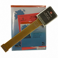
Manufacturer Part Number
PCM18XT0
Description
MODULE PROC PIC18F4685
Manufacturer
Microchip Technology
Datasheet
1.PCM18XT0.pdf
(484 pages)
Specifications of PCM18XT0
Accessory Type
Processor Module
Product
Microcontroller Modules
Core Processor
PIC18F4685
Lead Free Status / RoHS Status
Not applicable / Not applicable
For Use With/related Products
ICE2000
For Use With
ICE2000 - EMULATOR MPLAB-ICE 2000 POD
Lead Free Status / RoHS Status
Lead free / RoHS Compliant, Not applicable / Not applicable


11.0
The Timer0 module incorporates the following features:
• Software selectable operation as a timer or
• Readable and writable registers
• Dedicated 8-bit, software programmable
• Selectable clock source (internal or external)
• Edge select for external clock
• Interrupt-on-overflow
REGISTER 11-1:
© 2009 Microchip Technology Inc.
bit 7
Legend:
R = Readable bit
-n = Value at POR
bit 7
bit 6
bit 5
bit 4
bit 3
bit 2-0
counter in both 8-bit or 16-bit modes
prescaler
TMR0ON
R/W-1
TIMER0 MODULE
TMR0ON: Timer0 On/Off Control bit
1 = Enables Timer0
0 = Stops Timer0
T08BIT: Timer0 8-Bit/16-Bit Control bit
1 = Timer0 is configured as an 8-bit timer/counter
0 = Timer0 is configured as a 16-bit timer/counter
T0CS: Timer0 Clock Source Select bit
1 = Transition on T0CKI pin
0 = Internal instruction cycle clock (CLKO)
T0SE: Timer0 Source Edge Select bit
1 = Increment on high-to-low transition on T0CKI pin
0 = Increment on low-to-high transition on T0CKI pin
PSA: Timer0 Prescaler Assignment bit
1 = TImer0 prescaler is NOT assigned. Timer0 clock input bypasses prescaler.
0 = Timer0 prescaler is assigned. Timer0 clock input comes from prescaler output.
T0PS2:T0PS0: Timer0 Prescaler Select bits
111 = 1:256 Prescale value
110 = 1:128 Prescale value
101 = 1:64 Prescale value
100 = 1:32 Prescale value
011 = 1:16 Prescale value
010 = 1:8
001 = 1:4
000 = 1:2
T08BIT
R/W-1
T0CON: TIMER0 CONTROL REGISTER
Prescale value
Prescale value
Prescale value
W = Writable bit
‘1’ = Bit is set
R/W-1
T0CS
PIC18F2682/2685/4682/4685
R/W-1
T0SE
U = Unimplemented bit, read as ‘0’
‘0’ = Bit is cleared
R/W-1
The T0CON register (Register 11-1) controls all
aspects of the module’s operation, including the
prescale selection. It is both readable and writable.
A simplified block diagram of the Timer0 module in 8-bit
mode is shown in Figure 11-1. Figure 11-2 shows a
simplified block diagram of the Timer0 module in 16-bit
mode.
PSA
T0PS2
R/W-1
x = Bit is unknown
T0PS1
R/W-1
DS39761C-page 149
T0PS0
R/W-1
bit 0
Related parts for PCM18XT0
Image
Part Number
Description
Manufacturer
Datasheet
Request
R

Part Number:
Description:
Manufacturer:
Microchip Technology Inc.
Datasheet:
Part Number:
Description:
Manufacturer:
Microchip Technology Inc.
Datasheet:
Part Number:
Description:
Manufacturer:
Microchip Technology Inc.
Datasheet:
Part Number:
Description:
Manufacturer:
Microchip Technology Inc.
Datasheet:
Part Number:
Description:
Manufacturer:
Microchip Technology Inc.
Datasheet:
Part Number:
Description:
Manufacturer:
Microchip Technology Inc.
Datasheet:
Part Number:
Description:
Manufacturer:
Microchip Technology Inc.
Datasheet:
Part Number:
Description:
Manufacturer:
Microchip Technology Inc.
Datasheet: