PCM18XT0 Microchip Technology, PCM18XT0 Datasheet - Page 153
PCM18XT0
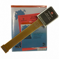
Manufacturer Part Number
PCM18XT0
Description
MODULE PROC PIC18F4685
Manufacturer
Microchip Technology
Datasheet
1.PCM18XT0.pdf
(484 pages)
Specifications of PCM18XT0
Accessory Type
Processor Module
Product
Microcontroller Modules
Core Processor
PIC18F4685
Lead Free Status / RoHS Status
Not applicable / Not applicable
For Use With/related Products
ICE2000
For Use With
ICE2000 - EMULATOR MPLAB-ICE 2000 POD
Lead Free Status / RoHS Status
Lead free / RoHS Compliant, Not applicable / Not applicable


12.0
The Timer1 timer/counter module incorporates these
features:
• Software selectable operation as a 16-bit timer or
• Readable and writable 8-bit registers (TMR3H
• Selectable clock source (internal or external) with
• Interrupt on overflow
• Module Reset on CCP1 Special Event Trigger
• Device clock status flag (T1RUN)
REGISTER 12-1:
© 2009 Microchip Technology Inc.
bit 7
Legend:
R = Readable bit
-n = Value at POR
bit 7
bit 6
bit 5-4
bit 3
bit 2
bit 1
bit 0
counter
and TMR3L)
device clock or Timer1 oscillator internal options
R/W-0
RD16
TIMER1 MODULE
RD16: 16-Bit Read/Write Mode Enable bit
1 = Enables register read/write of Timer1 in one 16-bit operation
0 = Enables register read/write of Timer1 in two 8-bit operations
T1RUN: Timer1 System Clock Status bit
1 = Device clock is derived from Timer1 oscillator
0 = Device clock is derived from another source
T1CKPS1:T1CKPS0: Timer1 Input Clock Prescale Select bits
11 = 1:8 Prescale value
10 = 1:4 Prescale value
01 = 1:2 Prescale value
00 = 1:1 Prescale value
T1OSCEN: Timer1 Oscillator Enable bit
1 = Timer1 oscillator is enabled
0 = Timer1 oscillator is shut off
The oscillator inverter and feedback resistor are turned off to eliminate power drain.
T1SYNC: Timer1 External Clock Input Synchronization Select bit
When TMR1CS = 1:
1 = Do not synchronize external clock input
0 = Synchronize external clock input
When TMR1CS = 0:
This bit is ignored. Timer1 uses the internal clock when TMR1CS = 0.
TMR1CS: Timer1 Clock Source Select bit
1 = External clock from pin RC0/T1OSO/T13CKI (on the rising edge)
0 = Internal clock (F
TMR1ON: Timer1 On bit
1 = Enables Timer1
0 = Stops Timer1
T1RUN
R-0
T1CON: TIMER1 CONTROL REGISTER
W = Writable bit
‘1’ = Bit is set
T1CKPS1
R/W-0
OSC
/4)
PIC18F2682/2685/4682/4685
T1CKPS0
R/W-0
U = Unimplemented bit, read as ‘0’
‘0’ = Bit is cleared
T1OSCEN
R/W-0
A simplified block diagram of the Timer1 module is
shown in Figure 12-1. A block diagram of the module’s
operation in Read/Write mode is shown in Figure 12-2.
The module incorporates its own low-power oscillator
to provide an additional clocking option. The Timer1
oscillator can also be used as a low-power clock source
for the microcontroller in power-managed operation.
Timer1 can also be used to provide Real-Time Clock
(RTC) functionality to applications with only a minimal
addition of external components and code overhead.
Timer1 is controlled through the T1CON Control
register (Register 12-1). It also contains the Timer1
Oscillator Enable bit (T1OSCEN). Timer1 can be
enabled or disabled by setting or clearing control bit,
TMR1ON (T1CON<0>).
T1SYNC
R/W-0
x = Bit is unknown
TMR1CS
R/W-0
DS39761C-page 153
TMR1ON
R/W-0
bit 0
Related parts for PCM18XT0
Image
Part Number
Description
Manufacturer
Datasheet
Request
R

Part Number:
Description:
Manufacturer:
Microchip Technology Inc.
Datasheet:
Part Number:
Description:
Manufacturer:
Microchip Technology Inc.
Datasheet:
Part Number:
Description:
Manufacturer:
Microchip Technology Inc.
Datasheet:
Part Number:
Description:
Manufacturer:
Microchip Technology Inc.
Datasheet:
Part Number:
Description:
Manufacturer:
Microchip Technology Inc.
Datasheet:
Part Number:
Description:
Manufacturer:
Microchip Technology Inc.
Datasheet:
Part Number:
Description:
Manufacturer:
Microchip Technology Inc.
Datasheet:
Part Number:
Description:
Manufacturer:
Microchip Technology Inc.
Datasheet: