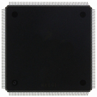
MCF5407AI220 Freescale Semiconductor, MCF5407AI220 Datasheet - Page 126

MCF5407AI220
Manufacturer Part Number
MCF5407AI220
Description
IC MPU 32B 220MHZ COLDF 208-FQFP
Manufacturer
Freescale Semiconductor
Series
MCF540xr
Specifications of MCF5407AI220
Core Processor
Coldfire V4
Core Size
32-Bit
Speed
220MHz
Connectivity
EBI/EMI, I²C, UART/USART
Peripherals
DMA, WDT
Number Of I /o
16
Program Memory Type
ROMless
Ram Size
4K x 8
Voltage - Supply (vcc/vdd)
1.65 V ~ 3.6 V
Oscillator Type
External
Operating Temperature
0°C ~ 70°C
Package / Case
208-FQFP
Maximum Clock Frequency
220 MHz
Operating Supply Voltage
1.8 V, 3.3 V
Maximum Operating Temperature
+ 105 C
Mounting Style
SMD/SMT
Minimum Operating Temperature
0 C
Program Memory Size
24KB
Cpu Speed
220MHz
Embedded Interface Type
I2C, UART
Digital Ic Case Style
FQFP
No. Of Pins
208
Supply Voltage Range
3.3V
Rohs Compliant
Yes
For Use With
M5407C3 - KIT EVAL FOR MCF5407 W/ETHERNET
Lead Free Status / RoHS Status
Lead free / RoHS Compliant
Eeprom Size
-
Program Memory Size
-
Data Converters
-
Lead Free Status / Rohs Status
Lead free / RoHS Compliant
Available stocks
Company
Part Number
Manufacturer
Quantity
Price
Company:
Part Number:
MCF5407AI220
Manufacturer:
freescaie
Quantity:
6
Company:
Part Number:
MCF5407AI220
Manufacturer:
Freescale Semiconductor
Quantity:
135
Company:
Part Number:
MCF5407AI220
Manufacturer:
FREESCALE
Quantity:
1 831
Company:
Part Number:
MCF5407AI220
Manufacturer:
Freescale Semiconductor
Quantity:
10 000
- Current page: 126 of 546
- Download datasheet (7Mb)
SRAM Operation
0-modulo-2K location in the 4-Gbyte address space and configured to respond to either
instruction or data accesses. Time-critical functions can be mapped into instruction
memory and the system stack. Other heavily-referenced data can be mapped into data
memory.
The following summarizes features of the MCF5407 SRAM implementation:
4.3 SRAM Operation
Each SRAM module provides a general-purpose memory block that the ColdFire processor
can access with single-cycle throughput. The location of the memory block can be specified
to any word-aligned address in the 4-Gbyte address space by RAMBARn[BA], described
in Section 4.4.1, “SRAM Base Address Registers (RAMBAR0/RAMBAR1).” The memory
is ideal for storing critical code or data structures or for use as the system stack. Because
the SRAM module connects physically to the processor’s high-speed local bus, it can
service processor-initiated accesses or memory-referencing debug module commands.
The Version 4 ColdFire processor core implements a Harvard memory architecture. Each
SRAM module may be logically connected to either the processor’s internal instruction or
data bus. This logical connection is controlled by a configuration bit in the RAM base
address registers (RAMBAR0 and RAMBAR1).
If an instruction fetch is mapped into the region defined by the SRAM, the SRAM sources
the data to the processor and any cache data is discarded. Likewise, if a data access is
mapped into the region defined by the SRAM, the SRAM services the access and the cache
is not affected. Accesses from SRAM modules are never cached, and debug-initiated
references are treated as data accesses.
Note also that the SRAMs cannot be accessed by the on-chip DMAs. The on-chip system
configuration allows concurrent core and DMA execution, where the core can reference
code or data from the internal SRAMs or caches while performing a DMA transfer.
4-2
• Two 2-Kbyte SRAMs, organized as 512 x 32 bits
• Single-cycle throughput. When the pipeline is full, one access can occur per clock
• Physical location on the processor’s high-speed local bus with a user-programmed
• Memory location programmable on any 0-modulo-2K address boundary
• Byte, word, and longword address capabilities
• The RAM base address registers (RAMBAR0 and RAMBAR1) define the logical
cycle.
connection to the internal instruction or data bus
base address, attributes, and access types for the two SRAM modules.
MCF5407 User’s Manual
Related parts for MCF5407AI220
Image
Part Number
Description
Manufacturer
Datasheet
Request
R
Part Number:
Description:
Mcf5407 Coldfire Integrated Microprocessor User
Manufacturer:
Freescale Semiconductor, Inc
Datasheet:
Part Number:
Description:
Manufacturer:
Freescale Semiconductor, Inc
Datasheet:
Part Number:
Description:
Manufacturer:
Freescale Semiconductor, Inc
Datasheet:
Part Number:
Description:
Manufacturer:
Freescale Semiconductor, Inc
Datasheet:
Part Number:
Description:
Manufacturer:
Freescale Semiconductor, Inc
Datasheet:
Part Number:
Description:
Manufacturer:
Freescale Semiconductor, Inc
Datasheet:
Part Number:
Description:
Manufacturer:
Freescale Semiconductor, Inc
Datasheet:
Part Number:
Description:
Manufacturer:
Freescale Semiconductor, Inc
Datasheet:
Part Number:
Description:
Manufacturer:
Freescale Semiconductor, Inc
Datasheet:
Part Number:
Description:
Manufacturer:
Freescale Semiconductor, Inc
Datasheet:
Part Number:
Description:
Manufacturer:
Freescale Semiconductor, Inc
Datasheet:
Part Number:
Description:
Manufacturer:
Freescale Semiconductor, Inc
Datasheet:
Part Number:
Description:
Manufacturer:
Freescale Semiconductor, Inc
Datasheet:
Part Number:
Description:
Manufacturer:
Freescale Semiconductor, Inc
Datasheet:
Part Number:
Description:
Manufacturer:
Freescale Semiconductor, Inc
Datasheet:


