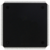
MCF5407AI220 Freescale Semiconductor, MCF5407AI220 Datasheet - Page 131

MCF5407AI220
Manufacturer Part Number
MCF5407AI220
Description
IC MPU 32B 220MHZ COLDF 208-FQFP
Manufacturer
Freescale Semiconductor
Series
MCF540xr
Specifications of MCF5407AI220
Core Processor
Coldfire V4
Core Size
32-Bit
Speed
220MHz
Connectivity
EBI/EMI, I²C, UART/USART
Peripherals
DMA, WDT
Number Of I /o
16
Program Memory Type
ROMless
Ram Size
4K x 8
Voltage - Supply (vcc/vdd)
1.65 V ~ 3.6 V
Oscillator Type
External
Operating Temperature
0°C ~ 70°C
Package / Case
208-FQFP
Maximum Clock Frequency
220 MHz
Operating Supply Voltage
1.8 V, 3.3 V
Maximum Operating Temperature
+ 105 C
Mounting Style
SMD/SMT
Minimum Operating Temperature
0 C
Program Memory Size
24KB
Cpu Speed
220MHz
Embedded Interface Type
I2C, UART
Digital Ic Case Style
FQFP
No. Of Pins
208
Supply Voltage Range
3.3V
Rohs Compliant
Yes
For Use With
M5407C3 - KIT EVAL FOR MCF5407 W/ETHERNET
Lead Free Status / RoHS Status
Lead free / RoHS Compliant
Eeprom Size
-
Program Memory Size
-
Data Converters
-
Lead Free Status / Rohs Status
Lead free / RoHS Compliant
Available stocks
Company
Part Number
Manufacturer
Quantity
Price
Company:
Part Number:
MCF5407AI220
Manufacturer:
freescaie
Quantity:
6
Company:
Part Number:
MCF5407AI220
Manufacturer:
Freescale Semiconductor
Quantity:
135
Company:
Part Number:
MCF5407AI220
Manufacturer:
FREESCALE
Quantity:
1 831
Company:
Part Number:
MCF5407AI220
Manufacturer:
Freescale Semiconductor
Quantity:
10 000
- Current page: 131 of 546
- Download datasheet (7Mb)
The MCF5407 implements a special branch instruction cache for accelerating branches,
enabled by a bit in the cache access control register (CACR[BEC]). The branch cache is
described in Section 2.1.2.1.1, “Branch Acceleration.”
The MCF5407 processor’s Harvard memory structure includes an 8-Kbyte data cache and
a 16-Kbyte instruction cache. Both are nonblocking and 4-way set-associative with a
16-byte line. The cache improves system performance by providing single-cycle access to
the instruction and data pipelines. This decouples processor performance from system
memory performance, increasing bus availability for on-chip DMA or external devices.
Figure 4-2 shows the organization and integration of the data cache.
Both caches implement line-fill buffers to optimize line-sized burst accesses. The data
cache supports operation of copyback, write-through, or cache-inhibited modes. A
four-entry, 32-bit buffer supports cache line-push operations, and can be configured to defer
write buffering in write-through or cache-inhibited modes. The cache lock feature can be
used to guarantee deterministic response for critical code or data areas.
A nonblocking cache services read hits or write hits from the processor while a fill (caused
by a cache allocation) is in progress. As Figure 4-2 shows, accesses use a single bus
connected to the cache.
All addresses from the processor to the cache are physical addresses. A cache hit occurs
when an address matches a cache entry. For a read, the cache supplies data to the processor.
For a write, which is permitted only to the data cache, the processor updates the cache. If
an access does not match a cache entry (misses the cache) or if a write access must be
written through to memory, the cache performs a bus cycle on the internal bus and
correspondingly on the external bus by way of the system integration module (SIM).
The SRAM module does not implement bus snooping; cache coherency with other possible
bus masters must be maintained in software.
Processor
ColdFire
Core
Control
Address
Data
Figure 4-2. Data Cache Organization
Directory Array
Address Path
Control Logic
Chapter 4. Local Memory
Cache
Data Path
Data Array
Address
Control
Data
Integration
System
Module
(SIM)
Cache Overview
Address/
External
Control
Data
Bus
4-7
Related parts for MCF5407AI220
Image
Part Number
Description
Manufacturer
Datasheet
Request
R
Part Number:
Description:
Mcf5407 Coldfire Integrated Microprocessor User
Manufacturer:
Freescale Semiconductor, Inc
Datasheet:
Part Number:
Description:
Manufacturer:
Freescale Semiconductor, Inc
Datasheet:
Part Number:
Description:
Manufacturer:
Freescale Semiconductor, Inc
Datasheet:
Part Number:
Description:
Manufacturer:
Freescale Semiconductor, Inc
Datasheet:
Part Number:
Description:
Manufacturer:
Freescale Semiconductor, Inc
Datasheet:
Part Number:
Description:
Manufacturer:
Freescale Semiconductor, Inc
Datasheet:
Part Number:
Description:
Manufacturer:
Freescale Semiconductor, Inc
Datasheet:
Part Number:
Description:
Manufacturer:
Freescale Semiconductor, Inc
Datasheet:
Part Number:
Description:
Manufacturer:
Freescale Semiconductor, Inc
Datasheet:
Part Number:
Description:
Manufacturer:
Freescale Semiconductor, Inc
Datasheet:
Part Number:
Description:
Manufacturer:
Freescale Semiconductor, Inc
Datasheet:
Part Number:
Description:
Manufacturer:
Freescale Semiconductor, Inc
Datasheet:
Part Number:
Description:
Manufacturer:
Freescale Semiconductor, Inc
Datasheet:
Part Number:
Description:
Manufacturer:
Freescale Semiconductor, Inc
Datasheet:
Part Number:
Description:
Manufacturer:
Freescale Semiconductor, Inc
Datasheet:


