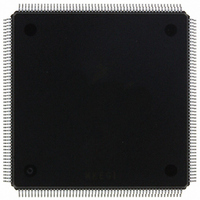
MCF5407AI220 Freescale Semiconductor, MCF5407AI220 Datasheet - Page 275

MCF5407AI220
Manufacturer Part Number
MCF5407AI220
Description
IC MPU 32B 220MHZ COLDF 208-FQFP
Manufacturer
Freescale Semiconductor
Series
MCF540xr
Specifications of MCF5407AI220
Core Processor
Coldfire V4
Core Size
32-Bit
Speed
220MHz
Connectivity
EBI/EMI, I²C, UART/USART
Peripherals
DMA, WDT
Number Of I /o
16
Program Memory Type
ROMless
Ram Size
4K x 8
Voltage - Supply (vcc/vdd)
1.65 V ~ 3.6 V
Oscillator Type
External
Operating Temperature
0°C ~ 70°C
Package / Case
208-FQFP
Maximum Clock Frequency
220 MHz
Operating Supply Voltage
1.8 V, 3.3 V
Maximum Operating Temperature
+ 105 C
Mounting Style
SMD/SMT
Minimum Operating Temperature
0 C
Program Memory Size
24KB
Cpu Speed
220MHz
Embedded Interface Type
I2C, UART
Digital Ic Case Style
FQFP
No. Of Pins
208
Supply Voltage Range
3.3V
Rohs Compliant
Yes
For Use With
M5407C3 - KIT EVAL FOR MCF5407 W/ETHERNET
Lead Free Status / RoHS Status
Lead free / RoHS Compliant
Eeprom Size
-
Program Memory Size
-
Data Converters
-
Lead Free Status / Rohs Status
Lead free / RoHS Compliant
Available stocks
Company
Part Number
Manufacturer
Quantity
Price
Company:
Part Number:
MCF5407AI220
Manufacturer:
freescaie
Quantity:
6
Company:
Part Number:
MCF5407AI220
Manufacturer:
Freescale Semiconductor
Quantity:
135
Company:
Part Number:
MCF5407AI220
Manufacturer:
FREESCALE
Quantity:
1 831
Company:
Part Number:
MCF5407AI220
Manufacturer:
Freescale Semiconductor
Quantity:
10 000
- Current page: 275 of 546
- Download datasheet (7Mb)
31–18
11.3.2.3 DRAM Controller Mask Registers (DMR0/DMR1)
The DRAM controller mask registers (DMR0 and DMR1), shown in Figure 11-4, include
mask bits for the base address and for address attributes.
Table 11-5 describes DMRn fields.
17–9
Reset
Bits
Field
Addr
Bits
5–4
3–2
1–0
R/W
8
7
31
Name
BAM
Name
WP
—
—
PM
PS
—
Figure 11-4. DRAM Controller Mask Registers (DMR0 and DMR1)
Base address mask. Masks the associated DACRn[BA]. Lets the DRAM controller connect to various
DRAM sizes. Mask bits need not be contiguous (see Section 11.5, “SDRAM Example.”)
0 The associated address bit is used in decoding the DRAM hit to a memory block.
1 The associated address bit is not used in the DRAM hit decode.
Reserved, should be cleared.
Write protect. Determines whether the associated block of DRAM is write protected.
0 Allow write accesses
1 Ignore write accesses. The DRAM controller ignores write accesses to the memory block and an
Reserved, should be cleared.
Port size. Determines the port size of the associated DRAM block. For example, if two 16-bit wide
DRAM components form one DRAM block, the port size is 32 bits. Programming PS allows the
DRAM controller to execute dynamic bus sizing for associated accesses.
00 32-bit port
01 8-bit port
1x 16-bit port
Page mode. Configures page-mode operation for the memory block.
00 No page mode
01 Burst page mode (page mode for bursts only)
10 Reserved
11 Continuous page mode
Reserved, should be cleared.
Table 11-4. DACR0/DACR1 Field Description (Continued)
address exception occurs. Write accesses to a write-protected DRAM region are compared in the
chip select module for a hit. If no hit occurs, an external bus cycle is generated. If this external bus
cycle is not acknowledged, an access exception occurs.
BAM
Chapter 11. Synchronous/Asynchronous DRAM Controller Module
Table 11-5. DMR0/DMR1 Field Descriptions
MBAR + 0x10C (DMR0), 0x114 (DMR1)
18 17
Uninitialized
R/W
Description
Description
—
9
WP — C/I AM SC SD UC UD V
8
7
Asynchronous Operation
6
5
4
3
2
1
11-7
0
0
Related parts for MCF5407AI220
Image
Part Number
Description
Manufacturer
Datasheet
Request
R
Part Number:
Description:
Mcf5407 Coldfire Integrated Microprocessor User
Manufacturer:
Freescale Semiconductor, Inc
Datasheet:
Part Number:
Description:
Manufacturer:
Freescale Semiconductor, Inc
Datasheet:
Part Number:
Description:
Manufacturer:
Freescale Semiconductor, Inc
Datasheet:
Part Number:
Description:
Manufacturer:
Freescale Semiconductor, Inc
Datasheet:
Part Number:
Description:
Manufacturer:
Freescale Semiconductor, Inc
Datasheet:
Part Number:
Description:
Manufacturer:
Freescale Semiconductor, Inc
Datasheet:
Part Number:
Description:
Manufacturer:
Freescale Semiconductor, Inc
Datasheet:
Part Number:
Description:
Manufacturer:
Freescale Semiconductor, Inc
Datasheet:
Part Number:
Description:
Manufacturer:
Freescale Semiconductor, Inc
Datasheet:
Part Number:
Description:
Manufacturer:
Freescale Semiconductor, Inc
Datasheet:
Part Number:
Description:
Manufacturer:
Freescale Semiconductor, Inc
Datasheet:
Part Number:
Description:
Manufacturer:
Freescale Semiconductor, Inc
Datasheet:
Part Number:
Description:
Manufacturer:
Freescale Semiconductor, Inc
Datasheet:
Part Number:
Description:
Manufacturer:
Freescale Semiconductor, Inc
Datasheet:
Part Number:
Description:
Manufacturer:
Freescale Semiconductor, Inc
Datasheet:


