MCF5407AI220 Freescale Semiconductor, MCF5407AI220 Datasheet - Page 470
MCF5407AI220
Manufacturer Part Number
MCF5407AI220
Description
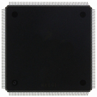
IC MPU 32B 220MHZ COLDF 208-FQFP
Manufacturer
Freescale Semiconductor
Series
MCF540xr
Specifications of MCF5407AI220
Core Processor
Coldfire V4
Core Size
32-Bit
Speed
220MHz
Connectivity
EBI/EMI, I²C, UART/USART
Peripherals
DMA, WDT
Number Of I /o
16
Program Memory Type
ROMless
Ram Size
4K x 8
Voltage - Supply (vcc/vdd)
1.65 V ~ 3.6 V
Oscillator Type
External
Operating Temperature
0°C ~ 70°C
Package / Case
208-FQFP
Maximum Clock Frequency
220 MHz
Operating Supply Voltage
1.8 V, 3.3 V
Maximum Operating Temperature
+ 105 C
Mounting Style
SMD/SMT
Minimum Operating Temperature
0 C
Program Memory Size
24KB
Cpu Speed
220MHz
Embedded Interface Type
I2C, UART
Digital Ic Case Style
FQFP
No. Of Pins
208
Supply Voltage Range
3.3V
Rohs Compliant
Yes
For Use With
M5407C3 - KIT EVAL FOR MCF5407 W/ETHERNET
Lead Free Status / RoHS Status
Lead free / RoHS Compliant
Eeprom Size
-
Program Memory Size
-
Data Converters
-
Lead Free Status / Rohs Status
Lead free / RoHS Compliant
Available stocks
Company
Part Number
Manufacturer
Quantity
Price
Company:

Part Number:
MCF5407AI220
Manufacturer:
freescaie
Quantity:
6
Company:
Part Number:
MCF5407AI220
Manufacturer:
Freescale Semiconductor
Quantity:
135
Company:
Part Number:
MCF5407AI220
Manufacturer:
FREESCALE
Quantity:
1 831
Company:
Part Number:
MCF5407AI220
Manufacturer:
Freescale Semiconductor
Quantity:
10 000


JTAG Register Descriptions
The IEEE Standard 1149.1 requires the EXTEST, SAMPLE/PRELOAD, and BYPASS
instructions. IDCODE, CLAMP, and HIGHZ are optional standard instructions that the
MCF5407 implementation supports and are described in the IEEE Standard 1149.1.
19.4.2 IDCODE Register
The MCF5407 includes an IEEE Standard 1149.1-compliant JTAG identification register,
IDCODE, which is read by the MCF5407 JTAG instruction encoded as octal 1.
(0000 for initial MCF5407 device)
Table 19-3 describes IDCODE bit assignments.
Instruction
19-6
31–28
27–22
21–12
11–1
0
BYPASS
31
CLAMP
Bits
(CMP)
(BYP)
Version Number
Version number. Indicates the revision number of the MCF5407
Design center. Indicates the ColdFire design center
Device number. Indicates an MCF5407
Indicates the reduced JEDEC ID for Motorola. Joint Electron Device Engineering Council (JEDEC)
Publication 106-A and Chapter 11 of the IEEE Standard 1149.1 give more information on this field.
Identifies this as the JTAG IDCODE register (and not the bypass register) according to the IEEE Standard
1149.1
30
Optional
Required
Class
29
110 Selects the bypass register and asserts functional reset while forcing all output and
111 Selects the single-bit bypass register, creating a single-bit shift register path from TDI
IR
Table 19-2. JTAG Instructions (Continued)
28
bidirectional pins configured as outputs to fixed, preloaded values in the
boundary-scan update registers. Enhances test efficiency by reducing the overall shift
path to one bit (the bypass register) while conducting an EXTEST type of instruction
through the boundary-scan register. CLAMP becomes active on the falling edge of
TCK in the Update-IR state when instruction-shift register data is equivalent to octal 6.
to the bypass register to TDO. Enhances test efficiency by reducing the overall shift
path when a device other than the MCF5407 is under test on a board design with
multiple chips on the overall 1149.1 defined boundary-scan chain. The bypass register
is implemented in accordance with 1149.1 so the shift register stage is set to logic 0
on the rising edge of TCK following entry into the capture-DR state. Therefore, the first
bit shifted out after selecting the bypass register is always a logic 0 (to differentiate a
part that supports an IDCODE register from a part that supports only the bypass
register).
BYPASS goes active on the falling edge of TCK in the Update-IR state when
instruction shift register data is equivalent to octal 7.
Table 19-3. IDCODE Bit Assignments
0 1 0 0 1 1 0 0 0 0 0 0 0 1 1 1 0 0 0 0 0 0 0 1 1 1 0 1
2
7
Figure 19-3. IDCODE Register
2
6
2
5
2
4
MCF5407 User’s Manual
2
3
2
2
2
1
2
0
Description
1
9
1
8
1
7
Description
1
6
1
5
1
4
1
3
1
2
1
1
1
0
9
8
7
6
5
4
3
2
1
0
Related parts for MCF5407AI220
Image
Part Number
Description
Manufacturer
Datasheet
Request
R

Part Number:
Description:
Mcf5407 Coldfire Integrated Microprocessor User
Manufacturer:
Freescale Semiconductor, Inc
Datasheet:
Part Number:
Description:
Manufacturer:
Freescale Semiconductor, Inc
Datasheet:
Part Number:
Description:
Manufacturer:
Freescale Semiconductor, Inc
Datasheet:
Part Number:
Description:
Manufacturer:
Freescale Semiconductor, Inc
Datasheet:
Part Number:
Description:
Manufacturer:
Freescale Semiconductor, Inc
Datasheet:
Part Number:
Description:
Manufacturer:
Freescale Semiconductor, Inc
Datasheet:
Part Number:
Description:
Manufacturer:
Freescale Semiconductor, Inc
Datasheet:
Part Number:
Description:
Manufacturer:
Freescale Semiconductor, Inc
Datasheet:
Part Number:
Description:
Manufacturer:
Freescale Semiconductor, Inc
Datasheet:
Part Number:
Description:
Manufacturer:
Freescale Semiconductor, Inc
Datasheet:
Part Number:
Description:
Manufacturer:
Freescale Semiconductor, Inc
Datasheet:
Part Number:
Description:
Manufacturer:
Freescale Semiconductor, Inc
Datasheet:
Part Number:
Description:
Manufacturer:
Freescale Semiconductor, Inc
Datasheet:
Part Number:
Description:
Manufacturer:
Freescale Semiconductor, Inc
Datasheet:
Part Number:
Description:
Manufacturer:
Freescale Semiconductor, Inc
Datasheet: