MCF5407AI220 Freescale Semiconductor, MCF5407AI220 Datasheet - Page 295
MCF5407AI220
Manufacturer Part Number
MCF5407AI220
Description
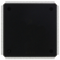
IC MPU 32B 220MHZ COLDF 208-FQFP
Manufacturer
Freescale Semiconductor
Series
MCF540xr
Specifications of MCF5407AI220
Core Processor
Coldfire V4
Core Size
32-Bit
Speed
220MHz
Connectivity
EBI/EMI, I²C, UART/USART
Peripherals
DMA, WDT
Number Of I /o
16
Program Memory Type
ROMless
Ram Size
4K x 8
Voltage - Supply (vcc/vdd)
1.65 V ~ 3.6 V
Oscillator Type
External
Operating Temperature
0°C ~ 70°C
Package / Case
208-FQFP
Maximum Clock Frequency
220 MHz
Operating Supply Voltage
1.8 V, 3.3 V
Maximum Operating Temperature
+ 105 C
Mounting Style
SMD/SMT
Minimum Operating Temperature
0 C
Program Memory Size
24KB
Cpu Speed
220MHz
Embedded Interface Type
I2C, UART
Digital Ic Case Style
FQFP
No. Of Pins
208
Supply Voltage Range
3.3V
Rohs Compliant
Yes
For Use With
M5407C3 - KIT EVAL FOR MCF5407 W/ETHERNET
Lead Free Status / RoHS Status
Lead free / RoHS Compliant
Eeprom Size
-
Program Memory Size
-
Data Converters
-
Lead Free Status / Rohs Status
Lead free / RoHS Compliant
Available stocks
Company
Part Number
Manufacturer
Quantity
Price
Company:

Part Number:
MCF5407AI220
Manufacturer:
freescaie
Quantity:
6
Company:
Part Number:
MCF5407AI220
Manufacturer:
Freescale Semiconductor
Quantity:
135
Company:
Part Number:
MCF5407AI220
Manufacturer:
FREESCALE
Quantity:
1 831
Company:
Part Number:
MCF5407AI220
Manufacturer:
Freescale Semiconductor
Quantity:
10 000


11.4.4.2 Interfacing Example
The tables in the previous section can be used to configure the interface in the following
example. To interface one 2M x 32-bit x 4 bank SDRAM component (8 columns) to the
MCF5407, the connections would be as shown in Table 11-31.
11.4.4.3 Burst Page Mode
SDRAM can efficiently provide data when an SDRAM page is opened. As soon as SCAS
is issued, the SDRAM accepts a new address and asserts SCAS every clock for as long as
accesses are in that page. In burst page mode, there are multiple read or write operations for
every
the associated SDRAM. The primary cycle of the transfer generates the
WRITE
the transfer completes, the
Note that in synchronous operation, burst mode and address incrementing during burst
cycles are controlled by the MCF5407 DRAM controller. Thus, instead of the SDRAM
enabling its internal burst incrementing capability, the MCF5407 controls this function.
This means that the burst function that is enabled in the mode register of SDRAMs must be
disabled when interfacing to the MCF5407.
Figure 11-18 shows a burst read operation. In this example, DACR[CASL] = 01, for an
SRAS-to-SCAS delay (t
MCF5407
Pins
Row
Column
SDRAM
Pins
MCF5407
Pins
Row
Column
SDRAM
Pins
Table 11-29. MCF5407 to SDRAM Interface (32-Bit Port, 11-Column Address Lines)
Table 11-30. MCF5407 to SDRAM Interface (32-Bit Port, 12-Column Address Lines)
SDRAM
Pins
MCF5407
Pins
ACTV
commands; secondary cycles generate only
A15 A14 A13 A12 A11 A10 A9 A17 A19 A21 A23 A24 A25 A26 A27 A28 A29 A30 A31
A15 A14 A13 A12 A11 A10
15
A0
A0
15
2
2
command in the SDRAM if the requested transfer size exceeds the port size of
A0
A15
A1
14
A1
14
3
3
A14
A2
13
A1
4
A2
13
4
Chapter 11. Synchronous/Asynchronous DRAM Controller Module
Table 11-31. SDRAM Hardware Connections
A3
12
A13
5
A3
A2
12
5
RCD
11
A4
PALL
6
A12
A4
11
A3
6
) of 2 CLKIN cycles. Because t
A5
10
7
A5
10
A11
command is generated to prepare for the next access.
7
A4
A6
9
8
A9
A6
9
8
A10
A5
A7
17
16
A17 A19 A21 A23 A25 A26 A27 A28 A29 A30 A31
A7
17
16
A6
A9
19
18
A8
A8
19
18
A17
A7
A9 A10 A11 A12 A13 A14 A15 A16 A17 A18
21
20
A9
21
20
READ
A18
23
22
A8
A10 A11 A12 A13 A14 A15 A16 A17
23
22
24
A19
or
A9
25
24
WRITE
RCD
25
A10 = CMD
26
is equal to the read CAS
26
A20
commands. As soon as
Synchronous Operation
27
27
ACTV
28
28
BA0
A21
and
29
29
READ
30
30
BA1
A22
11-27
31
31
or
Related parts for MCF5407AI220
Image
Part Number
Description
Manufacturer
Datasheet
Request
R

Part Number:
Description:
Mcf5407 Coldfire Integrated Microprocessor User
Manufacturer:
Freescale Semiconductor, Inc
Datasheet:
Part Number:
Description:
Manufacturer:
Freescale Semiconductor, Inc
Datasheet:
Part Number:
Description:
Manufacturer:
Freescale Semiconductor, Inc
Datasheet:
Part Number:
Description:
Manufacturer:
Freescale Semiconductor, Inc
Datasheet:
Part Number:
Description:
Manufacturer:
Freescale Semiconductor, Inc
Datasheet:
Part Number:
Description:
Manufacturer:
Freescale Semiconductor, Inc
Datasheet:
Part Number:
Description:
Manufacturer:
Freescale Semiconductor, Inc
Datasheet:
Part Number:
Description:
Manufacturer:
Freescale Semiconductor, Inc
Datasheet:
Part Number:
Description:
Manufacturer:
Freescale Semiconductor, Inc
Datasheet:
Part Number:
Description:
Manufacturer:
Freescale Semiconductor, Inc
Datasheet:
Part Number:
Description:
Manufacturer:
Freescale Semiconductor, Inc
Datasheet:
Part Number:
Description:
Manufacturer:
Freescale Semiconductor, Inc
Datasheet:
Part Number:
Description:
Manufacturer:
Freescale Semiconductor, Inc
Datasheet:
Part Number:
Description:
Manufacturer:
Freescale Semiconductor, Inc
Datasheet:
Part Number:
Description:
Manufacturer:
Freescale Semiconductor, Inc
Datasheet: