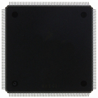
MCF5407AI220 Freescale Semiconductor, MCF5407AI220 Datasheet - Page 239

MCF5407AI220
Manufacturer Part Number
MCF5407AI220
Description
IC MPU 32B 220MHZ COLDF 208-FQFP
Manufacturer
Freescale Semiconductor
Series
MCF540xr
Specifications of MCF5407AI220
Core Processor
Coldfire V4
Core Size
32-Bit
Speed
220MHz
Connectivity
EBI/EMI, I²C, UART/USART
Peripherals
DMA, WDT
Number Of I /o
16
Program Memory Type
ROMless
Ram Size
4K x 8
Voltage - Supply (vcc/vdd)
1.65 V ~ 3.6 V
Oscillator Type
External
Operating Temperature
0°C ~ 70°C
Package / Case
208-FQFP
Maximum Clock Frequency
220 MHz
Operating Supply Voltage
1.8 V, 3.3 V
Maximum Operating Temperature
+ 105 C
Mounting Style
SMD/SMT
Minimum Operating Temperature
0 C
Program Memory Size
24KB
Cpu Speed
220MHz
Embedded Interface Type
I2C, UART
Digital Ic Case Style
FQFP
No. Of Pins
208
Supply Voltage Range
3.3V
Rohs Compliant
Yes
For Use With
M5407C3 - KIT EVAL FOR MCF5407 W/ETHERNET
Lead Free Status / RoHS Status
Lead free / RoHS Compliant
Eeprom Size
-
Program Memory Size
-
Data Converters
-
Lead Free Status / Rohs Status
Lead free / RoHS Compliant
Available stocks
Company
Part Number
Manufacturer
Quantity
Price
Company:
Part Number:
MCF5407AI220
Manufacturer:
freescaie
Quantity:
6
Company:
Part Number:
MCF5407AI220
Manufacturer:
Freescale Semiconductor
Quantity:
135
Company:
Part Number:
MCF5407AI220
Manufacturer:
FREESCALE
Quantity:
1 831
Company:
Part Number:
MCF5407AI220
Manufacturer:
Freescale Semiconductor
Quantity:
10 000
- Current page: 239 of 546
- Download datasheet (7Mb)
These registers are described in Section 8.5, “Programming Model.”
8.3 I
The I
For I
open collector outputs. (There is no such requirement for inputs.) The logic AND function
is exercised on both lines with external pull-up resistors.
Out of reset, the I
or responding to a slave transmit address, the I
receiver state. See Section 8.6.1, “Initialization Sequence,” for exceptions.
8.4 I
Normally, a standard communication is composed of the following parts:
1. START signal—When no other device is bus master (both SCL and SDA lines are
2. Slave address transmission—The master sends the slave address in the first byte
SCL
A
SDA
2
2
C compliance, all devices connected to these two signals must have open drain or
C module uses a serial data line (SDA) and a serial clock line (SCL) for data transfer.
START
Signal
at logic high), a device can initiate communication by sending a START signal (see
A in Figure 8-2). A START signal is defined as a high-to-low transition of SDA
while SCL is high. This signal denotes the beginning of a data transfer (each data
transfer can be several bytes long) and awakens all slaves.
after the START signal (B). After the seven-bit calling address, it sends the R/W bit
(C), which tells the slave data transfer direction.
2
2
AD7 AD6 AD5 AD4 AD3 AD2 AD1 R/W
C System Configuration
C Protocol
msb
1
The I
I
protocol, and restrictions, see The I
Version 2.1.
2
2
C bus protocol. For information on system configuration,
Calling Address
2
Figure 8-2. I
3
C default is as slave receiver. Thus, when not programmed to be a master
2
C module is designed to be compatible with the Philips
B
4
5
6
2
C Standard Communication Protocol
7
Chapter 8. I
R/W ACK
lsb
8
C
Bit
9
NOTE:
D
XXX
2
C Module
2
C module should return to the default slave
msb
D7 D6 D5
1
E
2
C Bus Specification,
2
3
Data Byte
D4 D3 D2 D1 D0
4
5
I
2
C System Configuration
6
7
lsb
8
ACK
No
Bit
9
STOP
Signal
F
8-3
Related parts for MCF5407AI220
Image
Part Number
Description
Manufacturer
Datasheet
Request
R
Part Number:
Description:
Mcf5407 Coldfire Integrated Microprocessor User
Manufacturer:
Freescale Semiconductor, Inc
Datasheet:
Part Number:
Description:
Manufacturer:
Freescale Semiconductor, Inc
Datasheet:
Part Number:
Description:
Manufacturer:
Freescale Semiconductor, Inc
Datasheet:
Part Number:
Description:
Manufacturer:
Freescale Semiconductor, Inc
Datasheet:
Part Number:
Description:
Manufacturer:
Freescale Semiconductor, Inc
Datasheet:
Part Number:
Description:
Manufacturer:
Freescale Semiconductor, Inc
Datasheet:
Part Number:
Description:
Manufacturer:
Freescale Semiconductor, Inc
Datasheet:
Part Number:
Description:
Manufacturer:
Freescale Semiconductor, Inc
Datasheet:
Part Number:
Description:
Manufacturer:
Freescale Semiconductor, Inc
Datasheet:
Part Number:
Description:
Manufacturer:
Freescale Semiconductor, Inc
Datasheet:
Part Number:
Description:
Manufacturer:
Freescale Semiconductor, Inc
Datasheet:
Part Number:
Description:
Manufacturer:
Freescale Semiconductor, Inc
Datasheet:
Part Number:
Description:
Manufacturer:
Freescale Semiconductor, Inc
Datasheet:
Part Number:
Description:
Manufacturer:
Freescale Semiconductor, Inc
Datasheet:
Part Number:
Description:
Manufacturer:
Freescale Semiconductor, Inc
Datasheet:


