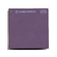
MC68040FE33A Freescale Semiconductor, MC68040FE33A Datasheet - Page 365

MC68040FE33A
Manufacturer Part Number
MC68040FE33A
Description
IC MICROPROCESSOR 32BIT 184-CQFP
Manufacturer
Freescale Semiconductor
Datasheet
1.MC68EC040FE33A.pdf
(442 pages)
Specifications of MC68040FE33A
Processor Type
M680x0 32-Bit
Speed
33MHz
Voltage
5V
Mounting Type
Surface Mount
Package / Case
184-CQFP
Package
184CQFP
Processor Series
M680xx
Core
CPU32
Lead Free Status / RoHS Status
Lead free / RoHS Compliant
Features
-
Lead Free Status / Rohs Status
Details
Available stocks
Company
Part Number
Manufacturer
Quantity
Price
Company:
Part Number:
MC68040FE33A
Manufacturer:
Freescale Semiconductor
Quantity:
10 000
- Current page: 365 of 442
- Download datasheet (4Mb)
A.2 INTERRUPT PRIORITY LEVEL (IPL2 –I PL0)
The IPL2–IPL0 pins do not have any affect on the selection of output buffer impedance.
A.3 JTAG SCAN (JS0)
The MC68040 DLE pin name has been changed to JS0. During normal operation, the JS0
pin cannot float, it must be tied to GND or Vcc directly or through a resistor. During board
testing, this pin retains the functionality of the JTAG scan of the MC68040 for compatibility
purposes. Refer to Section 6 IEEE 1149.1A Test Access Port (JTAG) for details concern-
ing IEEE 1149.1 Standard Test Access Port and Boundary Scan Architecture .
A.4 DATA LATCH AND MULTIPLEXED BUS MODES
The MC68LC040 does not implement the data latch or multiplexed modes of operation. The
CDIS pin is ignored at the rising edge of reset. All timing and drive capabilities of the
MC68LC040 are equivalent to those of the MC68040 in small output buffer impedance
mode.
A.5 FLOATING-POINT UNIT (FPU)
The FPU is not implemented on the MC68LC040. All floating-point instructions cause an
unimplemented floating-point exception to be taken with a new eight-word stack frame (for-
mat $4). The stack frame contains the status register (SR), program counter (PC), vector off-
set, effective address of the operand (where applicable), and PC value of the
unimplemented floating-point instruction.
A.5.1 Unimplemented Floating-Point Instructions and Exceptions
All legal MC68040 and MC68881/MC68882 floating-point instructions are defined as unim-
plemented floating-point instructions on the MC68LC040. These instructions generate a for-
mat $4 stack frame during exception processing before taking an F-line exception. These
instructions trap as an F-line exception, and the F-line exception handler can emulate them
in software to maintain user-object-code compatibility.
The MC68LC040 assists the emulation process by distinguishing unimplemented float-
ing-point instructions from other unimplemented F-line instructions. To aid emulation, the
effective address is calculated and saved in the format $4 stack frame. This simplifies and
speeds up the emulation process by eliminating the need for the emulation routine to deter-
mine the effective address and by providing information required to emulate the instruction
on the exception stack frame in the supervisor address space. However, the floating-point
instruction can reside in user space; therefore, the floating-point unimplemented exception
handler may need to access user instruction space. The following processing steps occur
for an unimplemented floating-point instruction:
MOTOROLA
1. When an unimplemented floating-point instruction is encountered, the instruction is
2. The processor waits for all previous integer instructions, write-backs, and associated
partially decoded, and the effective address is calculated, if required.
exception processing to complete before beginning exception processing for the un-
implemented floating-point instruction. Any access error that occurs in completing the
write-backs causes an access error exception, and the resulting stack frame indicates
Freescale Semiconductor, Inc.
For More Information On This Product,
Go to: www.freescale.com
M68040 USER’S MANUAL
MC68LC040
REV2.3 (01/29/2000)
A-5
Related parts for MC68040FE33A
Image
Part Number
Description
Manufacturer
Datasheet
Request
R

Part Number:
Description:
(MC600 Series) INTEGRATED CIRCUITS
Manufacturer:
ETC
Datasheet:
Part Number:
Description:
Manufacturer:
Freescale Semiconductor, Inc
Datasheet:
Part Number:
Description:
Manufacturer:
Freescale Semiconductor, Inc
Datasheet:
Part Number:
Description:
Manufacturer:
Freescale Semiconductor, Inc
Datasheet:
Part Number:
Description:
Manufacturer:
Freescale Semiconductor, Inc
Datasheet:
Part Number:
Description:
Manufacturer:
Freescale Semiconductor, Inc
Datasheet:
Part Number:
Description:
Manufacturer:
Freescale Semiconductor, Inc
Datasheet:
Part Number:
Description:
Manufacturer:
Freescale Semiconductor, Inc
Datasheet:
Part Number:
Description:
Manufacturer:
Freescale Semiconductor, Inc
Datasheet:
Part Number:
Description:
Manufacturer:
Freescale Semiconductor, Inc
Datasheet:
Part Number:
Description:
Manufacturer:
Freescale Semiconductor, Inc
Datasheet:
Part Number:
Description:
Manufacturer:
Freescale Semiconductor, Inc
Datasheet:
Part Number:
Description:
Manufacturer:
Freescale Semiconductor, Inc
Datasheet:
Part Number:
Description:
Manufacturer:
Freescale Semiconductor, Inc
Datasheet:
Part Number:
Description:
Manufacturer:
Freescale Semiconductor, Inc
Datasheet:


