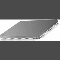
PC87393VJG National Semiconductor, PC87393VJG Datasheet - Page 110

PC87393VJG
Manufacturer Part Number
PC87393VJG
Description
IC, SUPER I/O DEVICE, TQFP-100
Manufacturer
National Semiconductor
Specifications of PC87393VJG
Data Rate
2Mbps
Supply Voltage Range
3V to 3.6V
Logic Case Style
TQFP
No. Of Pins
100
Operating Temperature Range
0°C to +70°C
Termination Type
SMD
Transceiver Type
Interface
Rohs Compliant
No
Available stocks
Company
Part Number
Manufacturer
Quantity
Price
Part Number:
PC87393VJG
Manufacturer:
NS/国半
Quantity:
20 000
www.national.com
7.0 X-Bus Extension
7.3.6
The read and write transactions in Latched address mode are similar to those used in Normal address mode, except for how
the addresses are placed on the X-Bus. In this mode, address signals 27-0 are output using the XA signals and via multi-
plexing over the data bus (XD7-0). Latch control signals XSTB2-0 help a system capture these signals. The XSTB2-0 signals
are placed as long as the address signal are valid (until the end of a transaction).
Once a read cycle on the LPC falls within the range of any of the enabled X-Bus decoded address ranges, a read cycle
begins. A read cycle starts by outputting the lower twenty address signals on address signals XA19-0, and address signals
27-20 on data signals XD7-0, on the rising edge of the clock. Two clock cycles later, a strobe signal (XSTB2) is asserted to
latch the information on an external latch. Two clock cycles later, a second set of address signals, 19-12, is placed on data
pins XD7-0. These may be latched using the strobe signal XSTRB1 output two cycles later on the rising edge of the clock.
Two clock cycles later, the last group of address signals, 11-4, is output on data signals XD7-0. The XSTRB0 output two
cycles later, on the rising edge of the clock, may be used to latch this part of the address. Two cycles later on the rising edge
of the clock, the PC8739x stops driving the data bus. At this point, all addresses are available either on the address outputs
of the PC8739x (XA19-0) or in one of the three latches. The system may require only part of these addresses, depending
on the size of the address memory or peripheral space. One clock cycle later, a chip select signal XCS1 or 0 is asserted,
based on the address accessed and the select signal mapping. From this point, the read continues as described for the Nor-
mal address mode. XSTRB2-0 are deasserted when the address becomes invalid.
Once a write cycle on the LPC falls within the range of any of the enabled decoded address ranges of the X-Bus functional
block, a read cycle is started. A write cycle starts by outputting the lower twenty address signals on address signals XA19-
0] and address signals 27- 20 on data signals XD7-0, on the rising edge of the clock. Two clock cycles later, a strobe signal
(XSTB2) is asserted to latch the information on an external latch. Two clock cycles later, a second set of address signals,
19-12, is placed on data pins XD7-0. These may be latched using the strobe signal XSTRB1 output two cycles later on the
rising edge of the clock. Two clock cycles later, the last group of address signals, 11-4, is output on the data signals XD7-0.
The XSTRB0 output, two cycles later on the rising edge of the clock, may be used to latch this part of the address. Two
cycles later on the rising edge of the clock, the PC8739x outputs the data signals on data pins XD7-0 on the rising edge of
the clock. At this point, all the address is available either on the address outputs of the PC8739x (XA[19:0]) or in one of the
three latches. The system may require only part of these addresses, depending on the size of the address memory or pe-
ripheral space. One clock cycle later, chip select signal XCS1 or 0 is asserted, based on the address accessed and the select
signal mapping. From this point, the write continues as described for the Normal address mode. XSTRB2-0 are deasserted
when the address becomes invalid.
CLK
(Internal for Reference)
XD7-0
XA19-0
XCS1-0
XWR
XRD
XRDY
Latched Address Mode X-Bus Transactions
(Continued)
Figure 25. Write Access Cycle - Normal Address Mode
Insert 12+”Programmed Wait States” of 33 MHz clocks here.
All non-clock signals remain the same during this inserted time.
110


