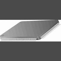
PC87393VJG National Semiconductor, PC87393VJG Datasheet - Page 47

PC87393VJG
Manufacturer Part Number
PC87393VJG
Description
IC, SUPER I/O DEVICE, TQFP-100
Manufacturer
National Semiconductor
Specifications of PC87393VJG
Data Rate
2Mbps
Supply Voltage Range
3V to 3.6V
Logic Case Style
TQFP
No. Of Pins
100
Operating Temperature Range
0°C to +70°C
Termination Type
SMD
Transceiver Type
Interface
Rohs Compliant
No
Available stocks
Company
Part Number
Manufacturer
Quantity
Price
Part Number:
PC87393VJG
Manufacturer:
NS/国半
Quantity:
20 000
- Current page: 47 of 148
- Download datasheet (703Kb)
2.0 Device Architecture and Configuration
2.11 FLOPPY DISK CONTROLLER (FDC) CONFIGURATION
2.11.1 General Description
The generic FDC is a standard FDC with a digital data separator, and is DP8473 and N82077 software compatible. The PC8739x
FDC supports 14 of the 17 standard FDC signals described in the generic Floppy Disk Controller (FDC) chapter, including:
Exceptions to standard FDC support include:
Table 16 lists the FDC functional block registers.
2.11.2 Logical Device 0 (FDC) Configuration
Table 17 lists the configuration registers which affect the FDC. Only the last two registers (F0h and F1h) are described here.
See Sections 2.2.3 and 2.2.4 for descriptions of the others.
FM and MFM modes are supported. To select either mode, set bit 6 of the first command byte when writing to/read-
ing from a diskette, where:
0 = FM mode
1 = MFM mode
A logic 1 is returned for all floating (TRI-STATE) FDC register bits upon LPC I/O read cycles.
Automatic media sense is supported by MSEN1-0 pins only on FDC signals routed to the PPM functional block (on
the Parallel Port)
DRATE1 is supported only on FDC signals routed to the PPM functional block (on the Parallel Port).
Index
30h
60h
61h
70h
71h
74h
75h
F0h FDC Configuration register
F1h Drive ID register
Activate. See also bit 0 of the SIOCF1 register and bit 0 of the SIOCF6 register. R/W
Base Address MSB register. Bits 7-3 (for A15-11) are read only, 00000b.
Base Address LSB register. Bits 2 and 0 (for A2 and A0) are read only, 00b.
Interrupt Number and Wake-Up on IRQ Enable register
Interrupt Type. Bit 1 is read/write; other bits are read only.
DMA Channel Select
Report no second DMA assignment
Offset
1. From the 8-byte aligned FDC base address.
00h
01h
02h
03h
04h
05h
06h
07h
Configuration Register or Action
1
Table 17. FDC Configuration Registers
Mnemonic
FIFO
DOR
MSR
DSR
CCR
SRA
SRB
TDR
DIR
Table 16. FDC Registers
Status A
Status B
Digital Output
Tape Drive
Main Status
Data Rate Select
Data (FIFO)
N/A
Digital Input
Configuration Control
47
(Continued)
Register Name
Type
R/W
R/W
R/W
RO
RO
W
W
R
X
R
Type
R/W
R/W
R/W
R/W
R/W
R/W
R/W
RO
Reset
00h
03h
F2h
06h
03h
02h
04h
24h
00h
www.national.com
Related parts for PC87393VJG
Image
Part Number
Description
Manufacturer
Datasheet
Request
R
Part Number:
Description:
National Semiconductor [8-Bit D/A Converter]
Manufacturer:
National Semiconductor
Datasheet:
Part Number:
Description:
National Semiconductor [Media Coprocessor]
Manufacturer:
National Semiconductor
Datasheet:
Part Number:
Description:
Digitally Controlled Tone and Volume Circuit with Stereo Audio Power Amplifier, Microphone Preamp Stage and National 3D Sound
Manufacturer:
National Semiconductor
Datasheet:
Part Number:
Description:
Digitally Controlled Tone and Volume Circuit with Stereo Audio Power Amplifier, Microphone Preamp Stage and National 3D Sound
Manufacturer:
National Semiconductor
Datasheet:
Part Number:
Description:
AC97 Rev 2 Codec with Sample Rate Conversion and National 3D Sound
Manufacturer:
National Semiconductor
Part Number:
Description:
Manufacturer:
National Semiconductor
Datasheet:
Part Number:
Description:
Manufacturer:
National Semiconductor
Datasheet:
Part Number:
Description:
General Purpose, Low Voltage, Low Power, Rail-to-Rail Output Operational Amplifiers
Manufacturer:
National Semiconductor
Datasheet:
Part Number:
Description:
8-bit 20 MSPS flash A/D converter.
Manufacturer:
National Semiconductor
Datasheet:
Part Number:
Description:
Low Noise Quad Operational Amplifier
Manufacturer:
National Semiconductor
Datasheet:
Part Number:
Description:
Quad Differential Line Receivers
Manufacturer:
National Semiconductor
Datasheet:
Part Number:
Description:
Quad High Speed Trapezoidal? Bus Transceiver
Manufacturer:
National Semiconductor
Datasheet:
Part Number:
Description:
Dual Line Receiver
Manufacturer:
National Semiconductor
Datasheet:
Part Number:
Description:
TTL to 10k ECL Level Translator with Latch
Manufacturer:
National Semiconductor
Datasheet:


