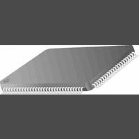
PC87393VJG National Semiconductor, PC87393VJG Datasheet - Page 60

PC87393VJG
Manufacturer Part Number
PC87393VJG
Description
IC, SUPER I/O DEVICE, TQFP-100
Manufacturer
National Semiconductor
Specifications of PC87393VJG
Data Rate
2Mbps
Supply Voltage Range
3V to 3.6V
Logic Case Style
TQFP
No. Of Pins
100
Operating Temperature Range
0°C to +70°C
Termination Type
SMD
Transceiver Type
Interface
Rohs Compliant
No
Available stocks
Company
Part Number
Manufacturer
Quantity
Price
Part Number:
PC87393VJG
Manufacturer:
NS/国半
Quantity:
20 000
- Current page: 60 of 148
- Download datasheet (703Kb)
www.national.com
2.0 Device Architecture and Configuration
2.15.6 GPIO Event Routing Register
This register enables the routing of the GPIO event to IRQ and/or SMI signals. It is implemented only for ports 0,1 which
have event detection capability. This register is reset by hardware to 00h.
Location:
Type:
Bit
Name
Reset
7-2
Bit
Bit
2
1
0
1
0
Pull-Up Control. This bit is used to enable/disable the internal pull-up capability of the corresponding GPIO pin.
It supports open-drain output signals with internal pull-ups and TTL input signals.
0: Disabled
1: Enabled (default)
Output Type. This bit controls the output buffer type (open-drain or push-pull) of the corresponding GPIO pin.
0: Open-drain (default)
1: Push-pull
Output Enable. This bit indicates the GPIO pin output state. It has no effect on the input path.
0: TRI-STATE (default)
1: Output enabled
Reserved
Enable SMI Routing
0: Disabled (default)
1: Enabled
Enable IRQ Routing
0: Disabled
1: Enabled (default)
Index F2h
R/W
7
0
6
0
5
0
Reserved
Description
Description
60
4
0
(Continued)
3
0
2
0
Enable SMI
Routing
1
0
Enable IRQ
Routing
0
1
Related parts for PC87393VJG
Image
Part Number
Description
Manufacturer
Datasheet
Request
R
Part Number:
Description:
National Semiconductor [8-Bit D/A Converter]
Manufacturer:
National Semiconductor
Datasheet:
Part Number:
Description:
National Semiconductor [Media Coprocessor]
Manufacturer:
National Semiconductor
Datasheet:
Part Number:
Description:
Digitally Controlled Tone and Volume Circuit with Stereo Audio Power Amplifier, Microphone Preamp Stage and National 3D Sound
Manufacturer:
National Semiconductor
Datasheet:
Part Number:
Description:
Digitally Controlled Tone and Volume Circuit with Stereo Audio Power Amplifier, Microphone Preamp Stage and National 3D Sound
Manufacturer:
National Semiconductor
Datasheet:
Part Number:
Description:
AC97 Rev 2 Codec with Sample Rate Conversion and National 3D Sound
Manufacturer:
National Semiconductor
Part Number:
Description:
Manufacturer:
National Semiconductor
Datasheet:
Part Number:
Description:
Manufacturer:
National Semiconductor
Datasheet:
Part Number:
Description:
General Purpose, Low Voltage, Low Power, Rail-to-Rail Output Operational Amplifiers
Manufacturer:
National Semiconductor
Datasheet:
Part Number:
Description:
8-bit 20 MSPS flash A/D converter.
Manufacturer:
National Semiconductor
Datasheet:
Part Number:
Description:
Low Noise Quad Operational Amplifier
Manufacturer:
National Semiconductor
Datasheet:
Part Number:
Description:
Quad Differential Line Receivers
Manufacturer:
National Semiconductor
Datasheet:
Part Number:
Description:
Quad High Speed Trapezoidal? Bus Transceiver
Manufacturer:
National Semiconductor
Datasheet:
Part Number:
Description:
Dual Line Receiver
Manufacturer:
National Semiconductor
Datasheet:
Part Number:
Description:
TTL to 10k ECL Level Translator with Latch
Manufacturer:
National Semiconductor
Datasheet:


