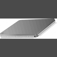
PC87393VJG National Semiconductor, PC87393VJG Datasheet - Page 85

PC87393VJG
Manufacturer Part Number
PC87393VJG
Description
IC, SUPER I/O DEVICE, TQFP-100
Manufacturer
National Semiconductor
Specifications of PC87393VJG
Data Rate
2Mbps
Supply Voltage Range
3V to 3.6V
Logic Case Style
TQFP
No. Of Pins
100
Operating Temperature Range
0°C to +70°C
Termination Type
SMD
Transceiver Type
Interface
Rohs Compliant
No
Available stocks
Company
Part Number
Manufacturer
Quantity
Price
Part Number:
PC87393VJG
Manufacturer:
NS/国半
Quantity:
20 000
5.0 Game Port (GMP)
The varying resistors R
directly by the horizontal and vertical positions, respectively, indicated by the game device. The waveform shaping circuits
are usually implemented outside the game device using constant resistors (R
with R
exact momentary position indicated by the game device.
When the Game Port is enabled and not in the midst of a game device position reading process, it drives the JOYnX,Y pins
low. In this state, the capacitors C
5.2.2
The process of capturing the position indicated by the game device is initiated by a command given to the Game Port to
release the JOYnX,Y lines, thus allowing the capacitors C
access to offset 1 from the Game Port base address, which is the offset of the Game Port Legacy Status Register (GMPLST,
see Section 5.3.3). Once JOYnX,Y pins are released, R
JOYnX,Y pins increases until it reaches V
The vertical and horizontal positions indicated by the game device are determined by measuring the time it takes for the
voltage level on the JOYnX,Y pins to reach the level of logic 1. Since the charging time is determined by the resistance val-
ues of R
indicated by the game device.
Once an axis pin is sensed as logic 1, the axis circuit discharge control is activated in order to discharge C
the corresponding axis pin to be driven low for approximately 1.5 sec. After that, this axis line is held low until another po-
sition reading process is initiated.
During the charge time and the 1.5 sec discharge time which follows, the corresponding axis line does not respond to any
reading process initiation. This prevents software from disturbing the position reading process and makes the position read-
ing processes of all axis lines independent of each other.
5.2.3
The button(s) status indication mechanism is described in Figure 16. Although this figure shows an active-low button
(R
button’s polarity.
BU0
>>R
VX/Y
Capturing the Position
VX/Y
Button Status Indication
BD0
, these components implement two R-C structures, the varying parameters of which are used to determine the
, measuring this time actually indicates the resistance values of R
), the polarity of the button can be either high or low, assuming that the Game Port software is aware of the
Game
Port
V
VX
Figure 15. Position Reading Process Waveform (not drawn to scale)
CX/Y
and R
V
V
Figure 16. Game Device Button Status Indication Mechanism
DD
IH
[V]
0
(Continued)
VY
X/Y
Buttons 0,1
Status
Indicators
Input Path
are usually implemented in the game device. Their resistance values are determined
Drive
Low
are completely discharged.
Idle
IH
. This process is described in Figure 15.
Time measured as
position indication
Release
Charge
CX/Y
X/Y
85
to be charged. This command is given by performing a write
and R
JOYnBTN0
JOYnBTN1
Discharge
Pins
VX/Y
start charging C
Drive
Low
Game Device Button Status Circuit
CX/Y
VX/Y
Idle
) and constant capacitors (C
, and therefore also reflects the position
RBU0
X/Y
, and the voltage level of the
Time
RBD0
X/Y
X/Y
. This causes
www.national.com
). Together


